


The 3D-Semiconductor Era
A deep dive

Introduction
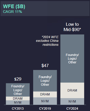
Semicap has been an attractive growth story over the last decade:
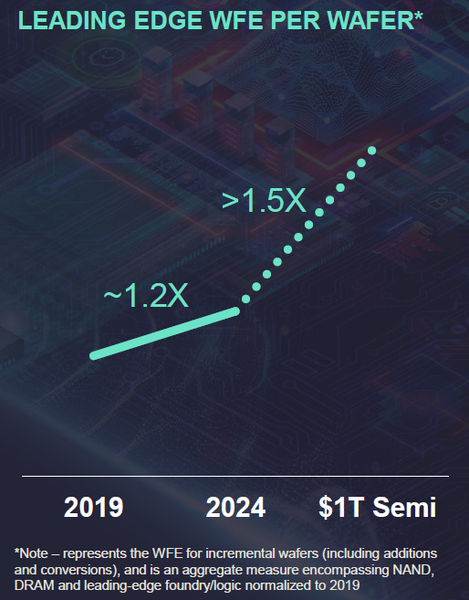
And the outlook continues to be attractive, as tool intensity to produce the most leading edge wafers will continue to increase:
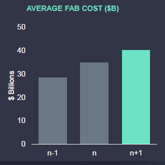
Which will raise the cost of a next-gen leading edge fab towards $40 billion:
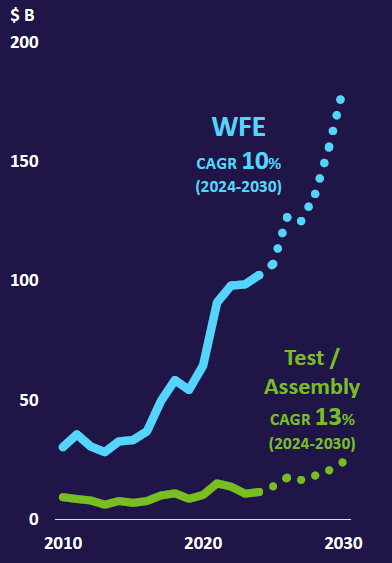
Tokyo Electron sees the WFE market growing at a 10% CAGR for the remainder of this decade (chart below). However, within the WFE market, certain segments are growing at faster CAGRs. These are the ones that will enable the coming technology inflections in chip architectures, which will be one of the key topics of today’s article. Due to the rise of heterogeneous integration, i.e. combining different types of dies into a single high-performance module, the assembly market is expected to grow at a faster CAGR of 13%:
The best example of heterogeneous integration are AI accelerators, where high-bandwidth DRAM dies are stacked on top of each other and subsequently interconnected with the most advanced GPU dies. AI accelerators are currently the pinnacle of semiconductor manufacturing, combining the most advanced front-end and back-end processes to create a state-of-the-art computing platform:
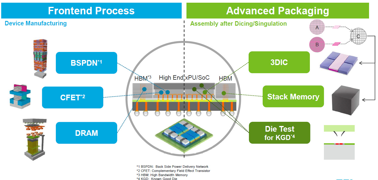
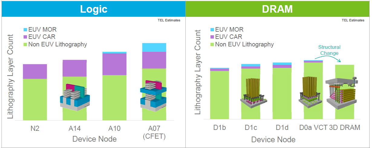
Today’s article will zoom in on the coming changes in the front-end processes and how these will impact the different wafer fabrication equipment (WFE) providers. A key part of the WFE industry is lithography, where ASML holds the monopoly. Tokyo Electron illustrates nicely how EUV intensity will continue to rise at the coming logic and DRAM nodes, i.e. the combination of the blue and purple bars on the charts below. However, once DRAM starts to move vertically, EUV intensity will drop:
This is one of the key trends in semi manufacturing which few ASML investors understand. ASML is a big play on scaling, i.e. transistor shrinkage, but as the industry will start to move inevitably in the vertical direction to construct advanced chips, this will be driven by different types of tools. So going vertical isn’t litho intensive, and also ASML is aware of this. This is the company’s CEO Fouquet explaining this at the recent investor day:
“When logic moves to gate-all-around (GAA), this requires some more lithography but those exposures will be done with DUV, not with EUV, because they are not critical. I'll give you another example. When NAND customers decide to make more layers, that requires more lithography. So we have seen the lithography number of layers for NAND go up over time. But again, that's not EUV at all. In this case, it's most probably KrF. So every time you have a change in architecture, this requires more processing steps. And steps that are not critical will be done with DUV. That's why you still see the number of DUV tools increasing and that's true for NAND, logic and DRAM.”
Even the coming FinFET to GAA transition isn’t EUV intensive, which is one of the reasons why ASML’s order flow has been fairly weak over the last six quarters or so. As the company wants the market to focus on its long term outlook rather than shorter term bookings which tend to be highly cyclical, ASML will stop reporting its order numbers going forward.
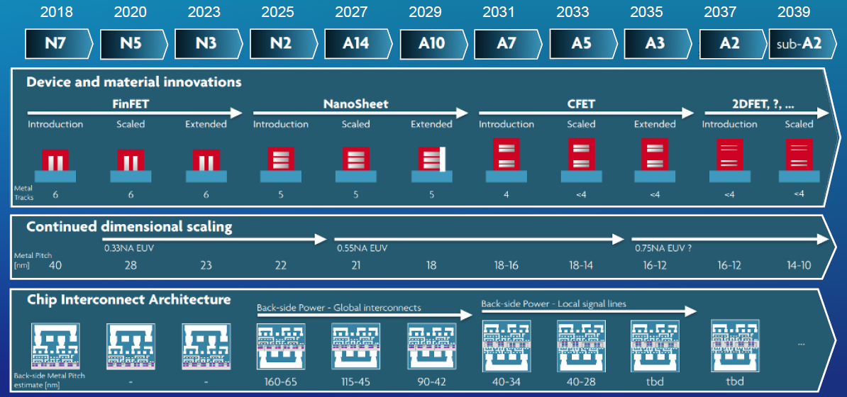
And the long term outlook is that after the GAA transition, subsequent nodes will see again a rising EUV intensity as scaling continues. And there is a very long roadmap in logic, which is good news for ASML as this is its key end market. The key to understand in the chart below is that the continued scaling of the metal pitch over the coming decade(s) will continue to increase EUV intensity:
While the memory industry’s move to 3D DRAM will be a negative for ASML, this transition will only come next decade and has been postponed several times already. This is the reason why ASML was keen to flag the ongoing hurdles to implement this new architecture at its recent investor day. The company is only seeing adoption of this new technology somewhere during the mid-2030s, which is a more conservative estimate than others in the semi industry such as Tokyo Electron.
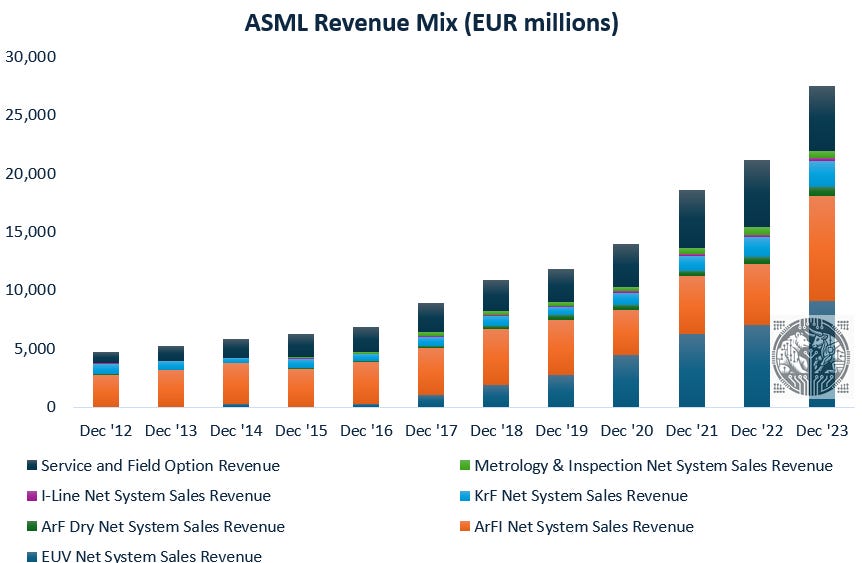
So the key problem for ASML is that while moving vertical in semi manufacturing still involves more lithography steps, these can be done with much lower priced tools. It’s really the building of smaller chip features that has to be done with the most advanced EUV tools, and these come at astronomical ASPs. And these have been the biggest driver of ASML’s revenue growth:
The bear case for ASML would be that fab yields will continue to drop at the most advanced nodes, making purchasing these wafers simply uneconomical. Samsung’s yields are already so terrible that they’ve lost practically all their customers. And also TSMC’s yields have been on the decline, although these remain sufficiently high so that customers can put in large orders for both N3 and N2. When yields decline too much, it doesn’t make sense to pay for that next-gen wafer as you can just order more wafers from the existing node. This still boosts your computing power as you can simply pack more dies together.
The other way to increase computing power is to start building vertically. Once your entire horizontal space is filled with the most advanced transistors, the obvious solution to add more in a single chip is to simply start stacking them on top of each other. Similar to how once all building space was taken up in Manhattan or Hong Kong, the obvious solution to house more people was to start building skyscrapers. We’re seeing the same in semiconductors and in NAND this is already well underway. This type of permanent memory currently has over 200 memory cell layers built on top of each other, a number which will continue to grow to over 1,000 in the coming decade.
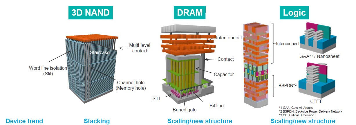
And also logic transistors are starting to integrate more 3D features. A GAA gate is constructed from three nanosheets stacked on top of each other and with a wrapping around each of these channels. Each of these layers has to be precisely constructed with advanced fab equipment, but as we saw above, this is not EUV intensive.
For premium subscribers, we’ll continue our story and we’ll do a deep dive on the coming technology inflections in leading edge semis, and on one semicap name which is strongly positioned to enable these. We’ll discuss the coming changes in memory (both NAND and DRAM) as well as in logic, and our name’s new innovations to unlock these roadmaps. Post this deep dive, we’ll do an analysis of the financials and valuation, where we see a long term IRR (annual total return) of 20-plus percent for this stock.