


Intel's fall & Gelsinger's master plan to take on TSMC
Outlook post foundry day

Intel’s fall
Intel has been on the ropes for a number of years now. Despite booms in semiconductor demand driven by the covid lockdowns and more recently, in the AI datacenter, the company failed completely to capitalize on these trends while profitability has actually been heading south. While Intel competes in a large variety of semiconductor end-markets, what currently remains in terms of profit generation is really a ‘90s-style desktop CPU business:
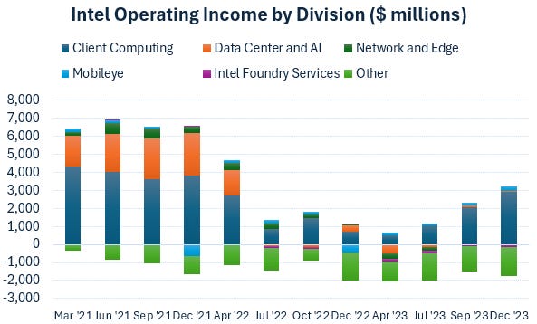
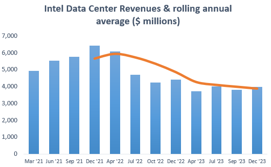
The big drama was the beating Intel has taken in the datacenter, where they went from a near monopoly position in x86 CPUs to a duopoly situation where AMD has consistently been gaining share:

Additionally, ARM-based CPUs are making headway in the datacenter as well, eroding the dominant position which the x86 architecture has enjoyed for decades. Large hyperscalers controlling the cloud market are increasingly designing their own silicon. There used to be a large barrier, as all software is designed to run on x86. However, as ARM’s IP has gradually been expanding beyond its stronghold in mobile, ever more software is becoming compatible with the architecture. Code written in major languages such as Java and Python now runs on top of ARM, and for other languages ever more compilers are becoming available as well. As the cloud market is dominated by a handful of players, hyperscalers can easily incentivize workloads to transition to their ARM-based silicon:
As a result of these drivers, further market share losses for Intel’s CPU business seem likely in the cloud. However, the company has been able to maintain a strong share in the enterprise datacenter market, partly thanks to its strong customer relationships. Basically, Intel sales people have been buying their customers lunch for the last twenty years, and as performance has been less of a factor in the decision making process for private datacenters, this helped Intel to maintain its position. Here’s AMD’s head of datacenter discussing these dynamics:
“In the cloud, it’s pretty simple, these guys are buying parts to power their business, their factory is their datacenter and so they are driving every bit of TCO (total cost of ownership) that is critically important. Almost nothing else matters. Once they know that you’re a reliable partner, whoever has got the best part wins. In enterprise, it’s a little bit more complicated. They’ve got long-standing relationships, you’ve got to educate a large number of customers. And so our ability to cover those end customers is one factor that somewhat limits our growth, and that’s somewhere we’ve been making investments. But you’ve also got the issue where the Intel sales guy has been buying lunch every quarter for the last 20 years, that factor also comes a little bit into play.”
Where did the problems start for Intel? Let’s step back to 2014, where things were looking pretty rosy still. Intel had been leading in process technology for decades and they were two to three years ahead of competition in terms of technology. TSMC’s and Samsung’s node labelling was also more aggressive, so a TSMC 10nm node for example was more comparable to Intel’s 14nm. However, it took Intel ages to get to 10nm and later on 7nm, while TSMC and Samsung moved swiftly to 10, 7, 5, and now 3nm.

In the meanwhile, competitor AMD laid out a clear roadmap for their CPU business. And as their partner TSMC delivered on the manufacturing side while AMD provided increasingly advanced designs, the company was an obvious market share winner.
Overall, it’s obvious that Intel was extremely poorly managed during these years and if CEO Krzanich had been there for much longer, I think the business might well have fully collapsed. However, a new hope is starting to emerge as Intel’s new management is extremely capable. Not least CEO Pat Gelsinger who has been reorganizing the internal incentive structures, for example by introducing competitive market forces to the various business units to improve decision making, optimize spending, and drive innovation. While Intel isn’t out of the woods yet, all indicators are now pointing in a positive direction and the company should at the very least be able to put up a much better fight versus its competition. On the positive, shareholders are also getting the optionality on a world-class foundry being built which should be able to compete with the likes of Samsung and TSMC in the long term.
Return of the jedi
Gelsinger previously already spent 30 years at Intel, from 1979 to 2009. At age 18, he started at Intel as a quality-control technician, pursuing in the meanwhile bachelor’s and master’s degrees in electrical engineering. Subsequently he rose through the ranks rapidly. In 1989 for example, he was the lead architect on the 486 processor, Intel’s key processor at the time. At age 32, he was named the youngest vice president in Intel’s history. In 2001, he already became the company’s CTO, overseeing the development of various technologies such as WiFi, USB, and Intel’s Core and Xeon processors. Gelsinger left the mothership in 2009 to become COO at EMC and in 2012, he made the move to take on the role of CEO at software firm VMware. As usual, his performance was excellent, he nearly tripled the company’s revenues and was named Best CEO by Glassdoor based on employee reviews.
As Intel was caught between a rock and a hard plate in the early ‘2020s, who could be better suited than Pat Gelsinger to steer this semiconductor powerhouse back on a positive trajectory? As such, in early 2021, Gelsinger was appointed as new CEO. Between the Krzanich and Gelsinger years, former CFO Swan took over for a few years, but he lacked the necessary technical expertise to really transform the former chip champion.

Moving at lightning speed
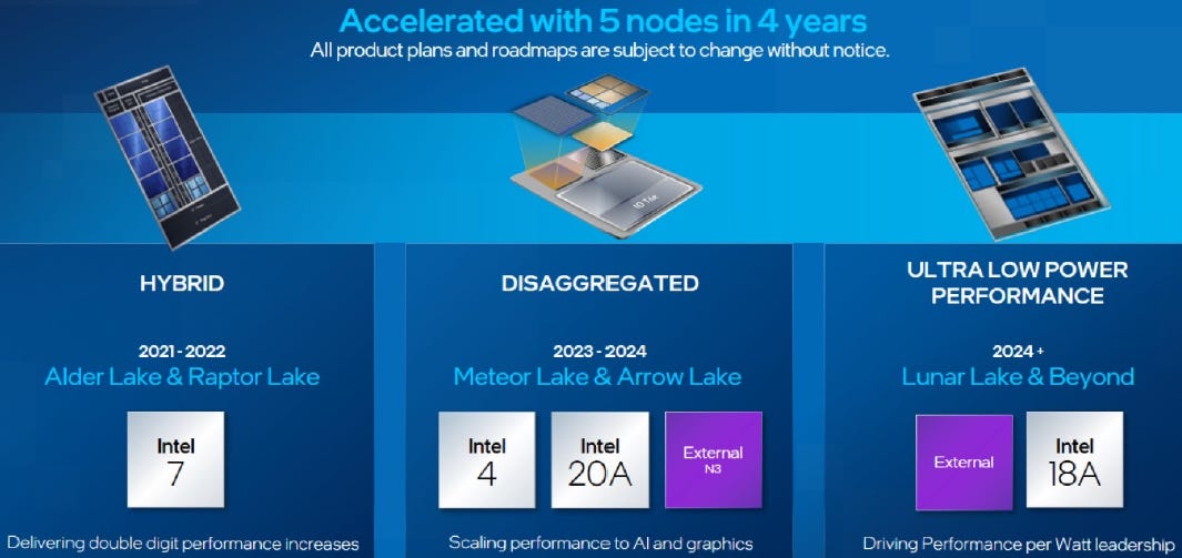
The key for Intel to once again become a successful semiconductor business is to regain process leadership, or at least to have a competitive node with TSMC. This is exactly what Gelsinger set out to do in early 2021. He laid out an ambitious plan to transition the company over 5 technology nodes in 4 years time, culminating in the regaining of process leadership at the company’s 18A node. This is Gelsinger updating the market on his plan during the recent call:
“First was the move into EUV, we began that with Intel 4 and 3. And those are done, high-volume manufacturing is underway. So we took the EUV risk off the table there. Then backside power, we ran an internal node, something we didn’t disclose to external foundry customers, but we ran many wafers using Intel 3 with backside power to de-risk before you put it into Intel 20A and 18A. And then, gate-all-around transistor. So 18A brings those two together, backside power and gate-all-around.
We are first in the industry to have incorporated both gate-all-around and backside power delivery in a single process node, and 2 years ahead of our competition. Arrow Lake, our lead Intel 20A vehicle will launch this year. Intel 18A is expected to achieve manufacturing readiness in the second half of '24, completing our five nodes in 4 years journey and bringing us back to process leadership. I am pleased to say that Clearwater Forest, our first Intel 18A product for servers has already gone into fab and Panther Lake for desktops will be heading there shortly.
As we’ve been going through the development process, backside power on 18A has been elegant, beautiful, high yield, very clean in its introduction. As customers are starting to look at that, they’re really seeing great benefits. In some cases, almost as much performance as significant area benefit.
We have begun installation of the industry's first High-NA EUV tool in our most advanced technology development site in Oregon, aimed at addressing challenges beyond 18A. We remain focused on being good stewards of Moore's Law and ensuring a continuous node migration path over the next decade and beyond. We came into 2023 committing to one 18A foundry customer, we executed on four, inclusive of a meaningful prepay and our momentum continues to grow.
Our advanced packaging business is proving to be yet another important advantage for IFS. During the quarter, we captured 3 additional advanced packaging design wins, bringing the total to 5 in 2023, with the majority of revenues starting in 2025. To support our growing demand, just yesterday, we opened Fab 9 in New Mexico, marking a milestone for high-volume 3D advanced packaging.
In total, across wafer and advanced packaging, our lifetime deal value for IFS is now over $10 billion, more than doubling from the $4 billion we provided in our last update.”
The momentum is clearly there, with Intel continuing to sign new deals for its fledgling foundry business. At the recent foundry day, the $10 billion pipeline was already raised to $15 billion, with customers including Microsoft, Mediatek and Valens Semi.

The five nodes in four years strategy is culminating into Intel retaking the lead in terms of innovation. We noted previously that TSMC will be moving more slowly to the latest innovations in leading edge semi architectures than its key challengers, Intel and Samsung. The current champion’s strategy is to remain on the FinFET architecture just a while longer at its N3 node, while moving to gate-all-around at N2 in 2025 and to backside power at N2P a year later. Meanwhile, Intel has a long history of implementing novel chip architectures as illustrated below:

This is TSMC’s CEO giving their view on process technology:
“Actually, we do not underestimate any of our competitors or take them lightly. Having said that, our internal assessment shows our N3P technology demonstrated comparable PPA to 18A competitors’ technology but with an earlier time to market, better technology, and much better cost. Our 2 nanometer technology without backside power is more advanced than both N3P and 18A, and will be the most advanced technology when it is introduced in 2025.”
There has been a bit of back and forth on this topic, with both companies claiming to have process leadership at its next nodes.
Intel 3 is basically Intel 4 but for foundry customers. So Intel 4 is manufacturing the company’s in-house semis, while Intel 3 will do so for the external fabless customers. Although the company will then later on bring its own volumes onto node 3 as well. Intel is using this similar strategy in 20A vs 18A, with 20A being ramped up with in-house designs and subsequently 18A becoming the bulk node, both for external foundry and internal business units. TSMC has somewhat of a similar strategy as they first scale up a new node with Apple’s orders, which is its largest customer, and which is then followed by a more diversified order flow of other leading edge customers.
Below is Gelsinger discussing Intel’s innovations with Ben Thompson of Stratechery:
“PowerVia (i.e. backside power), when you look at a metal stack of a modern process, leading edge technology might have fifteen to twenty metal layers. Metal one, metal two, and transistors all the way at the bottom. So it’s just an incredible skyscraper design. Well, the top level of metals is almost entirely used for power delivery, so now you have to take signals and weave them up through this lattice and then they’re screwing up your metal routing. So the idea of moving them to the bottom is magic. The first time I saw this laid out, as a former chip designer, I was like, “Hallelujah!”. Everybody loves this, and this is really an Intel innovation. The industry looked at this and said, “Wow, these guys are years ahead of anything else”, and now everybody else is racing to catch up while we’re already in our second and third generation here.
We also had a lot of pent-up innovation. We had congestion at the integration phase, but not at the invention phase. So I had a candy store of ideas like PowerVia. Now given enough capital, enough team, we were able to go quickly into it — bam, bam, bam. So you’re racing through capital very rapidly, you’re driving the development teams very aggressively. “Oh, you just got your breather on getting Intel 4 into production. Okay, you got six weeks to get the next one up and running and ready for the qualification process to start, and then we’re six months from right into 20A, and then six months later, right into 18A”. It’s an incredibly intense schedule, but we fell behind, we had to be intense, we had to really bet hard to make 18A the winner and every indication is, as I said, I’ve been looking at scanning electron microscope images for forty years, this is a work of art. I do think that there’s merit in some of the skepticism, “Hey, you fumbled last time, what have you done now?”. Well, I’ve changed the leadership, I’ve changed the development model, I’ve changed many of the people in it, and I’ve thrown incredible amounts of capital at this to go give them what they need.
At the same time, there’s a fundamental economic disadvantage to build in US or Europe and the ecosystem that has emerged in Asia, it’s lower cost. The CHIPS Act is designed to close those cost gaps and I’m not asking for handouts by any means, but I’m saying for me to economically build major manufacturing in US and Europe, those cost gaps must be closed, because if I’m going to plunk down $30 billion for a major new manufacturing facility and out of the gate, I’m at a 30%, 40% cost disadvantage. That’s what the CHIPS Act was about — if we want balanced, resilient supply chains, we must close that economic gap so that we can build in the US and Europe as we have been.”
IDM 2.0
Intel’s new business model is called ‘IDM 2.0’. The old and original business model was the traditional IDM model — i.e. integrated device manufacturer — basically a vertically integrated semiconductor manufacturer and designer. The modern semiconductor business model on the other hand is the separation between the foundry and the designer, the latter also known as the fabless company. A classic example of this modern approach is the Nvidia - TSMC relationship, where both sides can be hyper focused on their role in the value chain, i.e. designing GPUs in the case of Nvidia and manufacturing them on the latest process technologies in the case of TSMC.
What Intel is trying to accomplish here under the new IDM 2.0 model is to have the best of both worlds. The biggest change is that its manufacturing capabilities will be opened up to external customers, i.e. becoming a foundry, thereby propelling the manufacturing side to become much more efficient by introducing it to market forces. Intel’s manufacturing (the IFS division) will for the very first time be running its own P&L, generating revenues so that it can start optimizing a profit margin. Under the old model, manufacturing would purely be a cost center where the various Intel divisions such as client, datacenter and networking could allocate costs to.
An obvious big drawback of this old approach was that there was little attention paid towards optimizing this cost base. So divisions would often request hot lots to the manufacturing division — for example, to test out various new designs — forcing the fab to halt regular production and switch the process over to fulfill these urgent orders. Under the new system on the contrary with manufacturing having its own P&L, hot lots are priced at 1.5 to 3x the regular orders, so that the various Intel divisions can start optimizing their spending. For example, by placing these test orders when the fabs are less busy.
This is Intel’s CFO giving more details on the IDM 2.0 model at the foundry day last year:
“Today our manufacturing, technology development and IFS groups comprise roughly 40% of our headcount, 25% of our OpEx, and more than 90% of our CapEx. Yet our ability to benchmark and track the effectiveness of these investments has historically been obscured by the lack of transparency inherent in an allocated cost model.
Our pivot to giving manufacturing its own P&L is critical to identifying cost reductions. This new model will add transparency and comparability that exposes the true economics of the business by more directly measuring the financial performance of our teams with peers. We're already seeing benefits of this newfound transparency and accountability and expect to see many more as teams are incentivized to drive better financial performance.
Since our founding in 1968, we have been an integrated device manufacturer, a company that both designs and manufactures its own semiconductor chips. Intel was tremendously successful executing this strategy for many decades. We had two guiding principles for manufacturing under IDM 1.0. First, always maintain a capacity buffer given our strong market position and second, move to the next node as quickly as possible aligned with Moore's Law. Additional capacity was key as the cost of ceding market share outweighed the incremental capital cost. Unfortunately, this also had the unintended consequence that the business units could drive excessive expedited wafers and frequent changes to wafer loadings without economic consequence or accountability.
And we had a rapid ramp up and down approximately every two years, where cost reduction was largely achieved by moving to the next node versus optimizing costs on existing nodes. We had leadership in process technology of up to two years versus competition, that led to consistent gross margins in the 50% to 60% range. This was the right strategy for the time, and we were highly successful.
The semiconductor industry — and computing in general — has evolved rapidly. With the advent of smartphones, the digital network, the intelligent edge, cloud computing and AI, compute demands have diversified. The diversification of workloads and product lines led to the development of a vibrant foundry ecosystem. Furthermore, the industry is experiencing a significant increase in capital intensity as cutting-edge nodes grow more expensive. Finally, there is an ongoing technology pivot to disaggregation that will drive longer tails, as some IP will remain on older process technologies that doesn't require the shrink that would come from the next node. This increases the criticality of cost-optimizing existing nodes versus simply moving all capacity to the next node.
The IDM model provides four key advantages. First, it enables our technology development,manufacturing organization and business units to co-develop the process for custom product needs. Second, it enables us to get products to the market faster, Intel's internal CPUs are the ramp vehicle for Intel 18A, which will come to market in 2025 and enable us to regain process leadership. Third, the model gives us a substantial tailwind as an external foundry by ramping our process nodes on internal volume and de-risking the process for external customers. Lastly, under IDM 2.0, we will have an increased scale and a broader ecosystem of EDA, IP and design services that will further strengthen our capabilities.
As we transition to IDM 2.0, the manufacturing group will have a stand-alone P&L. Revenue will be based on wafer sales to the business units at market pricing, while costs will continue to be based on true manufacturing costs. As such, the manufacturing business will begin to generate a margin. The intercompany sale of wafers from the manufacturing P&L to business unit P&Ls will be eliminated, causing the Intel-level P&L to be consistent between IDM 1.0 and 2.0.
Pivoting from allocated cost to price will change behaviors within the business units. For example, it will encourage business units to move to the next node faster as they won't be burdened by the initial high cost as the new process ramps. It will also incentivize test time optimization, fewer expedited wafers and more selective use of samples as the business units see the direct impact of their choices hit their P&L.
The manufacturing group will now face the same market dynamics as their foundry counterparts. They will need to compete for volume through performance and price as internal customers will have the option to leverage third-party foundries. And to attract external foundry volume, they must do the same. This will lead to more effective adoption of standard third-party practices.
Leading fabless and foundry competitors combined into a virtual IDM would achieve roughly 70% gross margins, which is 20 to 30 points higher than Intel's recent results. Our long-term ambitions are to achieve non-GAAP 60% gross margins and 40% operating margins. It will take time before our manufacturing group P&L is world-class. We initially expect a negative operating margin percentage.”
Later on, we’ll go through Intel’s financial modelling but in the meanwhile, that leading gross margin they’re talking about of 70% looks high. Yes, Nvidia is currently generating 75% gross margins, but TSMC is only expected to generate 53%. So when you have a mix of these two businesses into one virtual IDM, you should get to a group gross margin of somewhere in the 60s.
Intel’s 60% gross margin target could be doable if the design businesses would be able to generate a 65% gross margin given their strongholds in enterprise and client CPUs, and then if the foundry could get above 50% like TSMC, we should be getting towards a group gross margin in the high 50s.
Note that IFS will have a lot of scale immediately, as Intel is still one of the largest semi designers in the world. Even today, Intel’s revenues are still comparable to those of Nvidia, with the former generating $54 billion in revenues over the last twelve months and the latter $61 billion.
This is the company’s vice president of corporate planning, Jason Grebe, going further into the IDM 2.0 model:
“While expedites provide faster routes for specific lots, they disrupt the efficiency of the factory network and lower the overall output, which leads to incremental capital and spending. Our benchmarking suggests that we expedite around 2 to 3x more than our industry peers with an estimated 8% to 10% hit in overall output.
In the internal foundry model, business units will be charged 1.5 to 3x the price of a wafer for expedited services, just like a customer would at an external foundry. As the number of expedite requests come down, the manufacturing group will be able to optimize their factory flows, and we estimate annual savings in the range of $500 million to $1 billion over time.
Next up is test and sort cost. As we shift to the internal foundry model, business units will now be charged the market price based on test time. Historically, Intel has enjoyed a structural cost advantage on its test platforms. This is driven by the high level of parallel testing we have spent years in developing. Currently, we estimate our test times are 2 to 3x those of our competitors. Effectively, our lower-cost testing platform was subsidizing the growth in our test times. By switching to the internal foundry model, we anticipate to save around $500 million annually over time.
Product business units will leverage stable pricing, which will help accelerate our ramp rates, leading to better capital utilization and faster yield curves. We estimate this will save up to $1 billion.
Overall, we estimate that the internal foundry model will help drive our overall $8 billion to $10 billion savings goal.
Everyone on this call knows that it is critical for our foundry business to be successful. We heard directly from our customers about what they need from us. Number one, a portfolio of process technology and IPs. Two, supply assurance. Three, protection of their data and IP. And four, world-class service levels.
Intel Foundry Services will have the authority to allocate corridors of capacity to its customers. We expect to be able to communicate clear supply commitments to our external customers. The next concern we hear is related to protection of customer data and IP. We will deliver complete segregation for foundry customers' data and IP. As we begin retooling the company for this transformation, we are architecting with a security-first mindset, with data separation as key in our systems design.”
The cost savings plan as we transition to IDM 2.0 is one of the key attractions for shareholders, as Intel is still burning large amounts of cash which we’ll get into. However, if $5 billion of cost savings can be achieved, that should allow the company to roughly break even in the coming years and possibly generate some positive FCFs.
Intel’s CFO gave us an update on this plan during the latest call:
“Every week that Pat and I spend on IFS, somebody brings up another big rock of savings that they can identify, because they are looking at the business in an entirely different way than they're used to looking at it. The product groups are now hyper-focused on test times, hot lots, and how much sample activity they use. And the factories are now hyper-focused on loadings and making sure they're properly thinking about their capital investment. So I think we'll get $4 billion to $5 billion of savings from this internal foundry model ultimately.”
Gelsinger convinces Pann to come out of retirement
Stuart Pann has a similar background as Gelsinger. Both studied electrical engineering and both have enjoyed decades-plus career trajectories at Intel.
Pann joined Intel in 1981, rising through the ranks and occupying a variety of management roles. And similar to Gelsinger, he also left Intel to take up a C-Suite position at another large US tech company. In Pann’s case, this was at HP, fulfilling the role of Chief Supply Chain Officer.
One of Gelsinger’s first actions was to bring Pann back to Intel to implement the IDM 2.0 model and since last year, to run the new IFS division. Pann gave a great presentation at the Goldman conference last year, a few highlights:
“Only by having process technology equivalency and then superiority do you actually make margin in this business. And we are on track to get to 5 nodes in 4 years.
To be successful in the foundry business, there are table stakes. You have to have competitive costs, competitive power, competitive scaling and a stable process road map. Without that, you can't play in this business. We have learned a lot over the last couple of years of how to go about doing that. And 18A, which is our leading-edge node, is the first process that we've designed from the ground up to have all those table stakes.
Job one this year is to go land 18A customers. We have landed and are working closely with MediaTek, we have landed a compute storage partner in Intel 3 and we have landed at least one prepay commitment. Cost, quality, performance, guarantees, collaboration, we put our best foot forward to go win MediaTek, and we learned a lot in that engagement process. A lot of my staff actually have come from foundry partners because we want to build that DNA inside of the organization. So we're looking at how do we make sure we've got a cohesive framework.
Where it hasn't worked out is people are just waiting to see what happens. They want to believe that 18A is going to be there. And so what they're saying, okay, I want to see a few more test chips or I want to see a more evolved PDK process design kit specification. I can tell you, all of them are interested in having Intel win. They're all interested in resilient supply chains.
We know that if we ever violate a customer's confidence, we're done in this business. Absolutely done. So we are religious about maintaining IP. Pat runs two separate staff meetings. I do not attend the business unit staff meetings anymore. We're creating two separate SAP instances to create these arm's length transactions, so nobody gets access to anybody else's data, we have firewalls. Our sales forces are separate. We have personal NDAs that our salespeople sign that there are consequences if they violate those NDAs.
What we are doing is, for any foundry deal, you have to commit capacity corridors. Once that's done, it's theirs. And our server and client businesses, they can't mess with it. Now we have to be really judicious about this.
We will sequence our construction spending based on commitments from customers and based on how well the client and server businesses are doing. Take all that, model it together, that gives you the construction schedule for Arizona, Ohio, Germany, Ireland and Israel.
This morning, we announced that we're an investor in ARM. So if you want to know that we're serious about embracing that world, which by the way, 80% of TSMC's wafers have an ARM processor in them. The fact that our organization is investing in ARM, doing partnerships with ARM, should give you a signpost that we're absolutely serious about playing in this business. If you're not working with ARM, you can't be a foundry's provider.
I have sitting here in my hand a single device on a single package. It's 100 billion transistors, it's 47 different tiles, all on one common substrate on the back here. It mixes Samsung HBM memory, TSMC-based technology and some of our compute technology. And this is the heart and soul of the Argonne supercomputer. You take 60,000 of these, another 20,000 Sapphires, and you have a machine that can do 2 exaFLOPs a second of compute performance. So that's 2 billion floating point operations a second. If you want to model the airflow across the wing, you can do that on a workstation. If you want to model the airflow across a plane, you do it on this. If you want to model fusion reactions, which are pretty tricky things to model, you do it on a device like this. If you want to model cancer curing drugs at the molecular level, you do it like this. It's 600 tons of compute, 4 tennis courts, the weight of an Airbus.
And the reason I bring this up in the context of packaging is this is sort of the acid test. If you can take 47 active tiles, mix and match this across different suppliers, have world-class back-end assembly test yields, this is why people are interested in talking to us about packaging technology. We've done some of the hardest packaging in the world.
If you look in the past, we were always returning 50% to 60% gross margins, but we were continually a process generation ahead. We have the roadmaps in place to do that with gate-all-around, with backside metallization. And hopefully, we're showing you enough in terms of sign posts, IP announcements, partnerships and prepays, that there is progress being made. I think Intel is hugely important to American manufacturing. I believe governments around the world view that. Certainly, the U.S. government views that.”

Intel’s recent foundry day
Intel held a foundry event last week and we’ll be going here through the highlights. First off, Pat Gelsinger talked about the geopolitical opportunity to shift manufacturing back to the US and Europe:
“COVID was a big wake-up call for us all, an auto factory building a $50,000 car being stopped for a $1 semiconductor. How did that happen? Semis, advanced computing is to the world's geopolitics what oil has been for the last 50 years. And silicon, fortunately, isn't restricted to where it's found. It's the second most abundant element on earth. But stunningly, in 1990, 80% of semiconductors were built in the U.S. and Europe. Today, 80% in a small concentrated area in Asia. We've seen this long, steady decline in terms of our supply chains for the world. Nothing should be reliant on a single place in the world. We need resilient access to supply chains and capacity, and thus the moonshot is 80-20 to 50-50 in a decade, rebalancing the supply chains of the world.”
Next up was Satya Nadella, Microsoft’s CEO, who highlighted these geographical concerns to be a key reason why they chose to produce a chip design on Intel’s leading 18A node. Pat Gelsinger continued on the progress they’re making in Moore’s law beyond 18A:
“So can I tell you more about what comes after 18A? Today, we are announcing Intel 14A for the first time. You can think about this like 1.4-nanometer technology, venturing deeply into the angstrom era. But we're also announcing that we're extending our nodes, adding P nodes, enhancements to existing nodes by adding performance capabilities. And new feature enhancements with E nodes. So we're filling out that full set of nodes in the road map.”
So Intel’s P nodes are basically enhanced compute performance whereas the E nodes improve efficiency. For 14A, the company is planning to make use of ASML’s latest high-NA tool:
")
Next up was Mediatek’s president of North America, one of the largest semi designers in the world with $14 billion in revenues last year, highlighting why they’ve chosen to work with IFS:
“So we look for capability and credibility, diversification and resiliency in the supply chain, and making sure there's a global footprint. So when you look at Intel Foundry, the credibility and capability was there. Intel has been investing in silicon manufacturing for well north of 50 years, and I think that provided a lot of confidence to the team.
MediaTek ships north of 2 billion chipsets every year. And we need somebody that can scale, and get a steady, competitive, and innovative supply of technology and components. As you know, we've got a long history of having a diverse supply base. And we push really hard on our partners, and we have high expectations. We felt that Intel could step up and meet and exceed those expectations.
The final thing that we looked at was ‘what else other than foundry could we get?’, i.e. packaging and substrate interconnect capabilities. And we think that with this partnership with Intel Foundry that we can accomplish our strategic goals.”
The foundry opportunity
So far Intel has secured a $15 billion pipeline for its IFS business. However, there is good reason to think that the company can do much better over the long term. Intel will be the first to deliver a node combining GAA and backside power, and with its process technology becoming at the very least competitive again with TSMC, there should be clear demand from fabless customers to also source advanced semiconductors from US soil.
As most will be aware, Taiwan is currently a geopolitical hot zone, with the two leading superpowers of today being bent on having the island within their respective spheres of influence. Naturally the US wants to see a democratic and Western-aligned government being in control of the island, whereas the CCP desires the island to become a Chinese province. Thus, we have a situation somewhat similar to the 3rd century BC, where the two superpowers in the Western Mediterranean at that time where vying for control of Sicily:

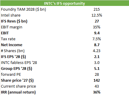
Below is a brief model on how much IFS could add to Intel’s group EPS. If the company can take a 12.5% market share in the external foundry market long term, say by 2028 - 2030, this business could contribute $2.1 in EPS for the group. And putting the combined group EPS on 28x, would give an IRR of 36%:
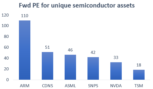
Now, this multiple is not overly bullish. If Intel could establish a successful leading edge foundry in the US, this would be a fairly unique asset in semiconductors. The trading forward PE multiple for these unique, high quality assets in semiconductors tends to be around 30 to 50x:
Whereas before Intel would always have to transition from node to node, which requires a lot of capex, the company now has a strategy to keep production capacity at previous nodes in place, so that customers can continue to design semis for these non-leading edge nodes. This is similar to TSMC where lagging nodes bring in substantial revenues:

For comparison, this is how Intel sees its node manufacturing profile evolving by wafer capacity:
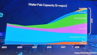
As wafers at more advanced nodes are priced much higher, the revenue profile will become much more skewed towards those very advanced nodes such as 18A and 14A.
The foundry business model on lagging nodes is attractive as once these assets are fully depreciated, they become high margin and thus EPS accretive. The downside is that these nodes can be more competitive, however, there are currently only three players below 10nm which will compete for Western fabless designs i.e. TSMC, Samsung, and Intel. I’m excluding SMIC here as this foundry is mainly attracting domestic Chinese designs, such as those of Huawei for example. However, as they are cut off from advanced equipment such as ASML’s EUV and immersion tools, they will find it extremely hard to compete at very advanced nodes. And it is also unlikely that US semi designers will source from them anyways.
The above TSMC chart also shows why it is difficult to break into the foundry market, as advanced nodes are only roughly 50% of TSMC revenues. That’s why I modelled in only a 12.5% share for Intel, as they can only start capturing share at these advanced nodes. Intel taking this amount of share in the overall market would imply a market share of around 28% in advanced foundries still, assuming the leading edge where Intel is competing will be around 45% of the market by 2028 - 2030.
This is not out of reach — the company has a $15 billion pipeline already, and assuming a lifetime of 3 years for these products, this would amount to $5 billion per annum in revenues. TSMC will make around $40 billion in advanced semis this year, so this would put Intel’s foundry already at around 12.5% the size of TSMC’s advanced fabs. So as Intel keeps executing and customers grow more comfortable with 18A and 14A, it is well possible that Intel could be moving to a share of over 25% of this market in the long term.
Intel has as drawback however that its other business units are directly competing with many of the leading edge semi designers. If I’m Jensen from Nvidia, am I really going to share my GPU designs with the same company that’s trying to disrupt me with their Gaudi GPUs? Even if you fully trust Intel’s internal walls, you’re still funding a direct competitor — the more cash Intel generates, the more they can increase their R&D budget to compete with you.
AMD has so far shown no interest to send volumes to their most direct competitor. Now potentially Apple could be interested, which is still TSMC’s largest client and is not really in competition with Intel. This should be big boon for Intel shareholders.
New datacenter CPUs
As discussed above, the cloud CPU market is where Intel has been losing share although they still have a stronghold in enterprise. This is Intel’s head of datacenter discussing the business last year:
“When looking at compute demand through the lens of the number of CPU cores delivered to the market, we have seen a mid-20s CAGR over the last 5 years and expect that pace of growth to continue. We expect x86 CPU revenue to follow core trends more closely than sockets in the coming years, and we are increasing the number of cores in our Xeon roadmap at a faster rate than in the past. Today's cloud businesses and the growth of microservices require higher core density at lower power.
Most AI workloads, such as data processing and analysis, are general-purpose workloads that run best on CPUs for several technical and economic reasons that include the ubiquity of the x86 architecture and the high TCO value of Xeon processors. Xeon also delivers exceptional compute for small- to medium-sized AI models that are under 10 billion parameters. These model sizes represent the volume of AI inference today. PyTorch 2.0 included a new compilation feature that we have optimized for CPU performance, yielding great results on many of the latest transformer models.
Our Xeon roadmap now has two swim lanes, our performance core or P-core Xeon processors are optimized to reduce TCO in both compute-optimized and general-purpose compute workloads. Our efficient core or E-core Xeon processors deliver best-in-class performance per watt with all the ecosystem advantages of the x86 instruction set.
Our fourth-gen Xeon processor, formerly codenamed Sapphire Rapids, launched earlier this year and is based on Intel 7 process technology. Customers are seeing gen-on-gen TCO improvements ranging from 52% to 66%.
Later this year, we expect to deliver our fifth-gen Xeon processor, Emerald Rapids. Silicon is coming out of our factories at very high quality, volume validation is well underway, and we're sampling the products to customers today. Our fifth-gen Xeon features an increase in processor cores and is pin-compatible with our fourth-gen Xeon, providing customers an easy migration path to take advantage of the processor's built-in workload accelerators, enhanced security features and increased performance. Customers who upgrade to fifth-gen Xeon require minimal validation, speeding up their time to deployment.
Following fifth-gen Xeon will be Granite Rapids and Sierra Forest. These two processors will be delivered on our next-generation high-performing platform, which shares the same base architecture and gives customers portability between the two products. The health of these two programs is excellent, we have narrowed our delivery window and will ship Sierra Forest to customers in the first half of 2024 with Granite Rapids following shortly after.
Granite Rapids delivers several improvements compared to the previous generation, including increased core counts, improved performance per watt, and faster memory and I/O innovations. We are building the fastest memory interface in the world. Intel invented and led the ecosystem in developing a new type of DIMM called multiplexer combined rank that lets us achieve speeds of 8,800 mega transfers per second based on DDR5. The innovation achieves an incredible 83% peak bandwidth increase over current gen server memory technology. This boost in bandwidth is critical for feeding the fast-growing core counts of modern CPUs. In fact, memory bandwidth is a first order performance limiter on many workloads, including those in the AI and HPC space.
Sierra Forest will be our first Xeon processor that leverages our efficient cores and will be our lead vehicle for the Intel 3 process. These processors will feature 144 E-cores per socket and will be highly competitive with high core count datacenter processors and ARM-based in-house developed solutions.
And announcing here for the first time, the follow on to Sierra Forest, a product we've codenamed Clearwater Forest, will come to market in 2025. Clearwater Forest will be manufactured on Intel 18A, the node where we plan to achieve process leadership.”
So the AI workloads she’s talking about is the pre-processing of the data, which comes before the training phase. Data scientists will analyze which factors will go into AI models, and how to transform these so that the AI can better work with them. A common transformation is to change a data column from absolute values to standard deviations for example. Although Nvidia has been moving into this area as well, they’ve enabled the popular Python Pandas library to run on their GPUs for example, which is usually used for these types of workloads together with NumPy.
So the company clearly has a strong roadmap of products on the leading process technologies they’ve been developing. This should at the very least put Intel in a much better competitive position to defend their share in the datacenter market. Whereas the enterprise market should remain solid, I expect the hyperscaler market to remain highly competitive, where the company will both have to compete with AMD and ARM-based custom silicon.
Overall, this is definitely not a business I would invest in stand-alone, as Intel’s market shares going forward will remain hard to predict.
Intel’s AI strategy
The company has a variety of GPU products targeted at AI acceleration in the datacenter. Flex GPUs are aimed at visual workloads such as media streaming and gaming, but can also be used for inferencing. Intel Max GPUs are used for physics and other scientific computations, while Gaudi is aimed at AI training and is thus meant to compete with Nvidia’s flagship GPUs such as the H100. Performance is not comparable to the H100, but Gaudi is much cheaper so on a TCO basis it still makes sense for some workloads.
The company is also developing its oneAPI computing platform to compete with Nvidia’s CUDA. The goal here is to easily run AI code in languages such as Python over Intel’s GPUs. Coverage for Intel’s CPUs is already great, all popular Python libraries will easily execute on these, but CPUs aren’t well suited for large LLM training and inferencing. Resulting in Nvidia capturing this market.
This is Pat Gelsinger updating us on this business during the latest call:
“We think more of the AI surge is going to result in AI inferencing on-prem, which we're well positioned to be a beneficiary. Here we are in year 20 of the public cloud and you have 60%-plus of compute in the cloud, but 80%-plus of data remains on-prem. Customers want to realize the value of that on-prem data with AI, and that's an enterprise strength for Intel.
As I finished probably 50 meetings between the World Economic Forum in Davos and CES with customers, I'll say we have an absolute unanimous response that they're going to be deploying a lot of their AI on-premise in their datacenters, and Xeons and our on-premise offerings are simply the preferred way for them to be taking advantage of those capabilities.
Obviously, we need to be participating more in the accelerator piece of that, and we're seeing the growing pipeline of our opportunities. Gaudi 3 is getting a lot of excitement. So we're going to be competing much more for that high-end accelerator footprint. But I think the message of 2024 is going to be AI inferencing everywhere: at the edge, on the AI PC, and it's going to be in the enterprise datacenter. All areas where Intel has a much stronger footprint.”
Intel’s bread-and-butter business, the PC and Notebook CPU market
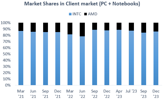
Finally, we get to Intel’s real core business, client CPUs. The company has been easily able to defend its positioning here, despite being on inferior process technologies than AMD:
I suspect the ‘Intel inside’ branding is still strong and most consumers just buy an Intel-based PC cause they know it works well. AMD on the other hand is a brand most consumers have never heard of.
And currently we’re getting into a situation where Intel will be much more competitive on process technology, resulting into a promising client product roadmap:
So it’s easy to be optimistic on this business, and share gains could actually well be on the table here. Additionally, we have revenues which look cyclically depressed and with the advent of the AI PC, there is scope for an upgrade cycle in the coming years combined with higher ASPs, as client CPUs will feature a NPU for LLM workloads.
Pat Gelsinger discussing their latest AI-enabled CPU:
“In Q4, we ushered in the age of the AI PC with the launch of Intel Core Ultra, representing our largest architectural shift in decades. The core Ultra is the most AI-capable and power-efficient client processor across CPUs, GPUs and NPUs. Ultra is the centerpiece of AI PC systems that are capable of natively running popular 10 billion parameter models, and drive superior performance on key AI-enhanced applications like Zoom, Adobe and Microsoft. We expect to ship approximately 40 million AI PCs in 2024 alone with more than 230 designs from ultra-thin PCs to handheld gaming devices.”
Financials — share price of $42.7 at time of writing, ticker INTC on the Nasdaq
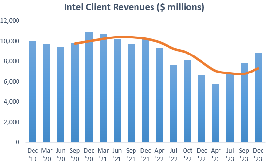
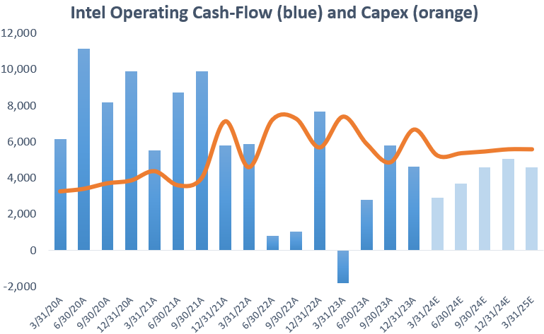
As a result of Intel’s struggles, operating cash flows have been heading south over the last two years with a true low point reacher during Q1 of ‘23 where the company managed to print a negative number, resulting in Intel burning an overall $9.2 billion during that quarter. Since then things have been gradually improving although capex remains elevated as the company is executing on the ambitious process technologies roadmap. You can also see that on the sell side’s estimates, the company is not expected to print a positive FCF number for the coming five quarters (light blue bars):
This is Pat Gelsinger discussing the outlook and business trends during the Q4 call:
“Discrete headwinds, including Mobileye, FPGAs and business exits, among others, are impacting overall revenue, leading to a lower Q1 guide. Importantly, we see this as temporary, and we expect sequential and year-on-year growth in both revenue and EPS for each quarter of fiscal year '24.
Our server business experienced solid sequential growth, consistent with market share, which we believe was flat with Q3 levels. Since launching 4th Gen Xeon in early 2023, we have shipped more than 2.5 million units with approximately one-third of all 4th Gen demand driven by AI. With our 5th Gen Xeon launch, we enable up to 42% higher AI inference performance. 5th Gen Xeon is on track to ship with OEMs next month.
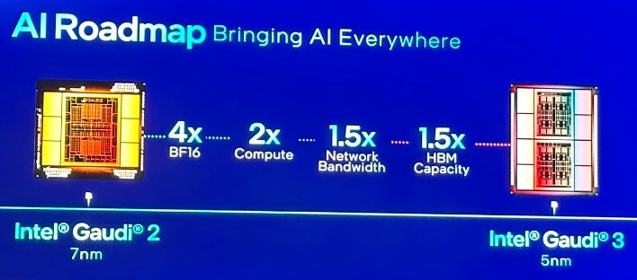
Our Gaudi 2 AI accelerators continue to demonstrate price performance leadership compared to the most popular GPUs. And a recent blog published by Databricks, Gaudi 2 was shown to clearly deliver the best training and inference performance per dollar based on public cloud pricing. We're building on this momentum with Gaudi 3, which is on track to launch this year and is expected to deliver performance leadership with 4x the processing power and double the networking bandwidth for greater scale outperformance. Our accelerated pipeline for 2024 grew double digits sequentially in Q4 and is now well above $2 billion and growing.
PSG (Programmable Solutions) is in the midst of an industry-wide cyclical correction for FPGAs, which we expect to last through the first half of '24. Operational momentum is strong and PSG executed its most ambitious FPGA roadmap, delivering 21 new product releases in 2023.
NEX (Network and Edge) is also driving the shift of AI networking in the cloud from proprietary technologies to open Ethernet-based approaches. NEX Q4 results beat our internal forecast and the division is poised for solid growth in 2024 across edge and network products, more skewed to the second half.”
A lot of semi companies have been citing weakness in automotive, industrial and FPGAs, so it’s no surprise this is impacting Intel’s FPGA business as well. Also, Q1 is usually the weakest quarter, so a weak guide here is not overly concerning.
Intel’s CFO added some details:
“While we expect a slightly subseasonal first quarter from our core product businesses, we see material inventory corrections in Mobileye and PSG (FPGAs).
With market signals remaining positive for PC demand and usage rates, we expect the TAM to grow in the low single digits in 2024.
We expect Q1 Data Center revenue to decline double-digit percent sequentially before improving through the year. While the Data Center has seen some wallet share shift between CPU and accelerators over the last several quarters, we expect growth in CPU compute cores to return to more normal historical rates and our discrete accelerator portfolio — with well over $2 billion in pipeline — to gain traction as we move through 2024.
Within NEX, telco markets are likely to remain weak through the year, though we expect solid growth from our network and edge products.
We're confident we can grow earnings faster than revenue this year and maintain roughly breakeven on adjusted free cash flow, though I'll remind you that the rapid pace of delivering 5 nodes in 4 years and capacity expansion in support of external foundry commitments remain headwinds on the pace of our margin expansion.”
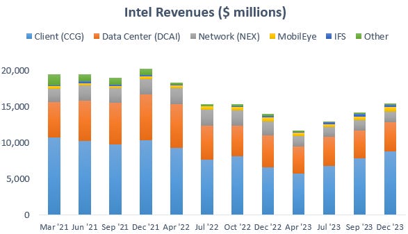
So bringing this all together, we have the below current revenue split. Over the coming years, client should be going into a cyclical upswing again — also driven by AI PC ASPs — and while currently datacenter budgets have been highly focused on GPUs, this brings substantial potential for CPU spend to recover in the coming years. So I actually think Intel’s revenue outlook for the coming years should be decent.
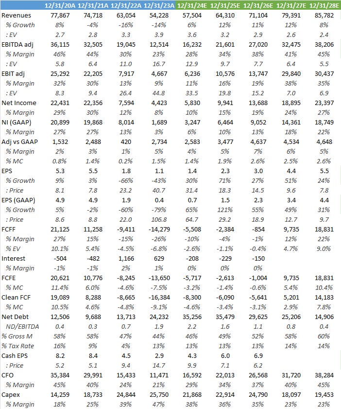
Below is how the sell side is modelling the business going forward. Wall Street is bullish on top line growth returning for Intel combined with margin improvements due to cost rationalization. The company is targeting $8 to $10 billion of annual cost savings exiting ‘25 and as the ambitious node ramping costs normalize. This should result in the company becoming FCF-positive once again by 2026-2027, generating a FCF yield of around 5% as capex normalizes.
Obviously these numbers are optimistic and due to the current cash burn of around $2 billion per quarter, I would point out that these shares remain risky, although the company still has $25 billion of cash on the balance sheet with the potential to float another $18 billion of Mobileye, which would be an easy way to raise cash. So this is not a business which is going to run out of cash anytime soon.
Management is more optimistic on bringing capex down, this is Intel’s CFO at the foundry day last year:
“We still believe the investment phase of Intel, which is kind of the '22 - '24 timeframe, we'll roughly be spending a net CapEx intensity in the 30s as a percent of revenue. And we still feel like confident that we will be able to modify that thereafter into a level that's somewhere in the mid-20s as a percent of revenue.”
Obviously this would be great as it would allow the business to already turn FCF-positive again by ‘25, bringing in an additional $6 billion of FCF. This would result in an overall FCF of $4-5 billion on consensus numbers, giving investors a 2 to 2.5% yield on the current market cap.
To summarize, the outlook for Intel is definitely much better than it was a few years ago. Now that the company is competitive again on process technology, there is potential for the datacenter business to improve, both on the CPU and GPU sides, as well as in networking. Additionally, the client and FPGA businesses are cyclically depressed, and with the launch of the AI PC, there is an obvious path for a recovery in client over the coming years. As a final positive, the successful building out of an advanced foundry business would be a clear catalyst for these shares to become a multibagger. Winning volumes from Apple for example would be very lucrative. However, I do suspect that most leading edge designers will remain with TSMC, rather than sharing their designs and directly funding Intel, who’s still a large competitor to most of the leading edge fabless players. In the meanwhile, the company’s financials remain not for the faint-hearted. There is an obvious risk that capex will remain elevated for quite some time to come, with the risk that the recovery in operating cash-flows won’t be sufficient to turn the business FCF-positive again, leading to shareholders having their cash burned over the coming years. The leading edge semi industry remains a highly competitive field and the rewards are great for those companies that get it right. While those who don’t, frequently never come back.
What do you think about Intel? Let me know in the comments section!
If you enjoy research like this, hit the like & restack buttons, and subscribe if you haven’t done so yet. Also, please share a link to this post on social media or with others who might be interested, it will help the publication to grow.
I’m also regularly discussing tech and investments on my Twitter.
Disclaimer - This article is not a recommendation to buy or sell the mentioned securities, it is purely for informational purposes. While I’ve aimed to use accurate and reliable information in writing this, it can not be guaranteed that all information used is of this nature. The views expressed in this article may change over time without giving notice. The future performance of the mentioned securities remains uncertain, with both upside as well as downside scenarios possible.


Excellent article, very well structured, detailed, and written!
Wow. Super research and writing!