


Chiplets, ASIC accelerators, and One Leading Edge Small Cap Play
Key trends in the data center space & one deep dive

Chiplets & ASIC Accelerators
As Moore’s Law—the historical trend where the amount of transistors in a chip area has been doubling every two years—slowed down, the semi industry started looking for other ways to continue to drive down the cost per transistor.
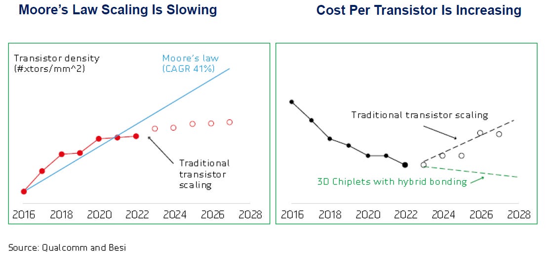
The solution was fairly simple—integrate more dies into a single computing system to boost computing power and to yield cost advantages in manufacturing. AMD has really been at the forefront of this trend, while also Intel is known to have some of the best advanced packaging capabilities. Nvidia by comparison, has been a laggard in these techniques and only joined two split dies together in its latest Blackwell GPU:
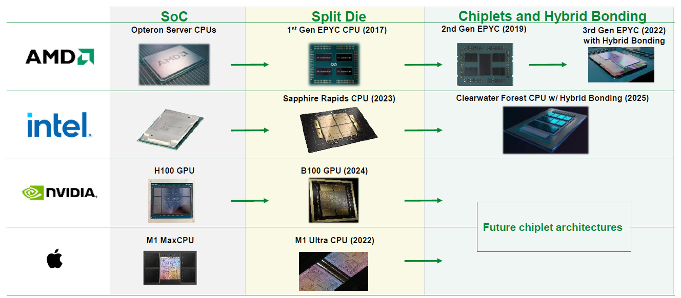
AMD’s MI300 is a marvel of packaging engineering, integrating dies horizontally via a joined interposer as well as vertically with advanced bonding tech:

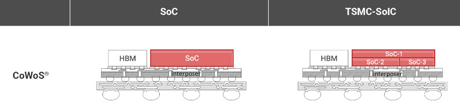
TSMC illustrates the packaging solutions they offer to realize such a computing system—CoWoS is used for the interposer integration while SoIC takes care of the vertical integration:
At the same time, ASICs continue to take share in the data center semi market. We discussed earlier this month how the hyperscaler CPU market is commoditizing due to software abstraction layers such as Kubernetes as well as other container orchestration platforms. This is a problem for both AMD and Intel, as it will result in a continued erosion of market share of their CPUs in the public clouds as well as other hyperscaler data centers.

Hyperscalers are aiming to deploy a similar strategy when it comes to GPUs in the AI server market. While Nvidia still dominates, there is an opening for ASICs to be deployed for more specialized workloads over time. For example, Meta can deploy a specialized chip to handle its ranking and recommendation algorithms for its social media feeds, while Google is running specialized silicon for its Youtube video workloads. Electricity is the highest cost to operate a design center and ASICs can give the hyperscaler a massive advantage in power consumption. For example, Meta’s MTIA v2 consumes only 90 Watts compared to the 700 Watts of an Nvidia H100. Naturally, you get 5 to 45 times more performance with an H100—depending on the floating point format—but if you don’t need such a power hungry chip for your ad algorithms, you just run it over MTIA and save a lot of money.

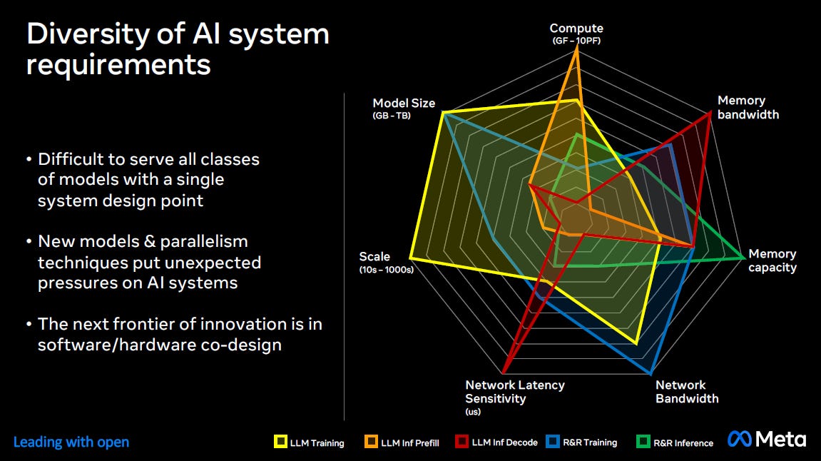
Meta also illustrates how a single system design cannot efficiently serve all workloads. For example, training requires more networking bandwidth while inference requires more memory capacity and memory bandwidth:
This is the reason why Nvidia has been building software so that its GPUs in a single node can easily be reoriented towards different tasks. This is Jensen discussing their new Dynamo orchestration layer at GTC:
“NVLink gives us the ability to take all of those GPUs and turn them into one massive GPU, the ultimate scale-up. Now that everything is on NVLink, I can disaggregate the prefill from the decode. I could decide that I want to use more GPUs for prefill and less for decode because I'm thinking a lot, I'm reading a lot of information or I'm doing deep research. On the other hand, when you're chatting with a chatbot and millions of us are doing the same thing, it is very token generation heavy and so it's very decode heavy. And so depending on the workload, we might decide to put more GPUs into decode or more GPUs into prefill.”
So Meta and the other hyperscalers’ strategy is to build differentiated software on top of commoditized hardware to scale their data centers:
And this can be accomplished by writing the needed software abstraction layers, something which all the hyperscalers are extremely good at:
However, in AI, we’re not there yet. As with most new innovations, the first waves of growth are driven by a vertically integrated solution i.e. the combination of hard- and software from a single provider. A good recent example here is Apple which kickstarted the smartphone industry. Its operating system can only run on the company’s own phones and chips, and the company even owns tools and the process IP at some of its manufacturing partners. Obviously, the extent of the company’s vertical integration is extreme. Later on, competitors started breaking up parts of this value chain—so Samsung focused on smartphone manufacturing while Google provided the open Android operating system.
We will see a similar battle play out in the AI data center market in the coming decade. With Nvidia being the vertically integrated Apple of the AI market, and competing computing platforms running on a variety of other accelerators looking to take share.
One certainty is that all this hardware will be running on chiplets. To design custom silicon, a global chiplets market is emerging where you can purchase a die off-the-shelf to integrate it into your computing module. This way, you can focus on designing your key silicon which you need to customize for your workloads. For example, you might decide to purchase an I/O die to handle the data traffic to your customly designed dies.
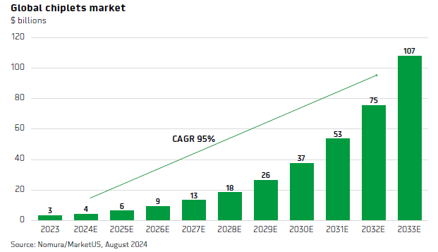
There is little doubt that both custom silicon as well as chiplets will be attractive growth markets over the coming five and ten years. For premium subscribers, we’ll take a close look at a leading edge, small cap player exposed to both these key trends. It’s a hardcore semi engineering firm working with several hyperscalers, and with obviously a lot of potential upside if things go right. There have been lots of success stories in companies that emerged to provide leading edge silicon and solutions to the hyperscaler market. But this isn’t easy, you need a team of highly talented and skilled engineers, as both niche know-how and the required investment capital form effective barriers to prevent these markets from becoming commoditized. So typically, there are not that many players in silicon which can effectively compete at the leading edge..