
Atomic layer deposition, next-gen transistors, and ASM
And more - including epitaxy and the semi cycle
Atomic layer deposition and next-gen transistors
In semiconductor manufacturing, deposition are the steps where thin films of material are popped onto the wafer to form gates, insulators and interconnections. Atomic layer deposition (ALD) is the most precise of these techniques as deposition layers can be build up atom by atom, giving fine-grained control on the exact thickness and composition of the film. Naturally this is great, but the drawback is that the process is slower and hence more costly. However due to Moore’s law, with transistor features scaling down into dimensions of countable nanometers, demand for ALD has been given a strong boost. As well as with transistor architectures going 3D. As these remain the two biggest trends in semiconductor advancements, probably together with 2.5 and 3D packaging, ALD is a natural area to look for exposure for tech investors. ASM International (ASMI or ASM for short) is at the center of this technology with a 55% global market share having been a pioneer in the field. And it remains really the company’s core bread-and-butter business contributing over 50% of revenues.
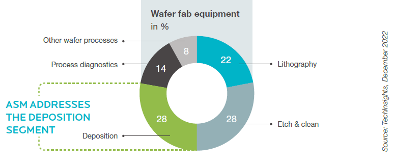
Deposition, etch and lithography are the three largest areas for semi tooling capex by the fabs:
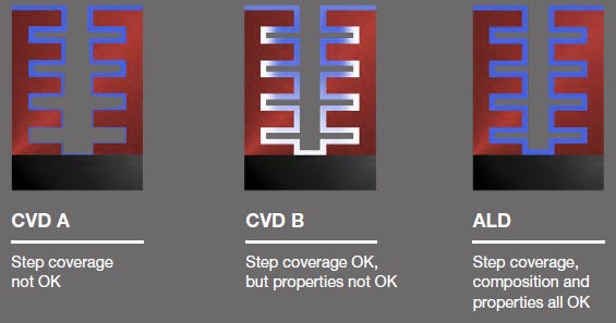
An illustration of how ALD can more precisely coat chip structures such as 3D NAND compared to chemical vapor deposition (CVD):
Starting from 45nm transistors, demand for ALD really took off with the introduction of the high-k metal gate transistor architecture (HKMG). Demand increased further with the transition to FinFETs, a 3D transistor architecture which was introduced by Intel at 22nm. The next generation will be an even more elegantly designed 3D transistor named gate all around (GAA), and this one will see its introduction at Samsung’s 3nm node. TSMC will be moving to GAA at 2nm, sticking with FinFETs for the moment. As more precise fabrication steps are needed to build GAA transistors, once again this will stimulate the demand for ALD.
Lam Research illustrates more clearly the various components in these types of transistors such as the gate, the source, and the drain. The silicon between the source and drain is called the channel and if a charge is running through the channel (controlled by the gate), this means the transistor is on. On versus off transistors can be represented in maths as ones versus zeros. For example, 1001 would mean transistor one and four are on, with number two and three being off. This would be an extremely simple four bit system. However, it illustrates the basics of computation on a mechanical system which has been miniaturized into a chip since the late sixties.
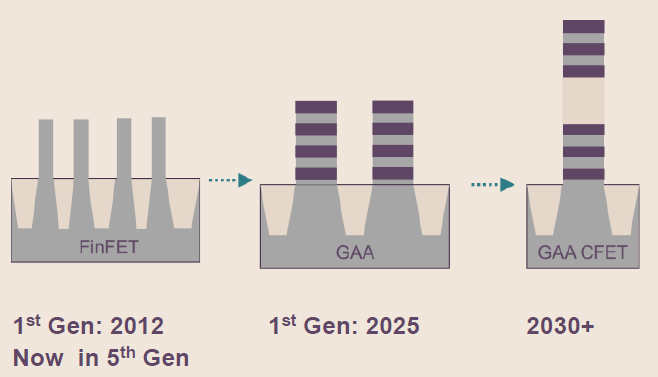
Next generation transistors afterwards such as CFET will require again more ALD steps, good news for ASM. A CFET is basically two GAAs stacked on top of each other:
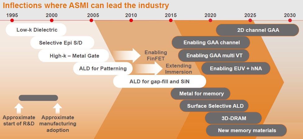
ASM’s CTO detailed this at the ‘21 capital markets day: “What’s more important to realize is that high k metal gate, it would not have been done without ALD. There would be no FinFET. At that time, EUV was not ready. We were ready to step in with ALD and do double patterning spaces, blocking layers and so on. So we extended immersion until EUV was mature enough. Now we are capturing layers where we need to support the EUV introduction, because the resistor is going to get a lot thinner and that means we have to drive new materials also in the patterning steps. And then transitioning to gate all around, these are 2D, very flat, very thin materials, and we apply them in a 3D structure. So this transition is of similar magnitude as the high-k metal gate transition. DRAM will move to high-k metal gate and later maybe to FinFET. It is going to follow the same trend as NAND, which went from planar to 3D. So if I summarize this, almost everything is going to 3D to enable scaling. We see a lot more thin films, complex stacks and more complex materials — and that requires more ALD.”
ASM’s head of products added some color: “The growth in ALD has increased a lot. This really reminds me of my days in the mid 1990s as a process engineer in CVD. During those days, CVD was growing in the same way. So the late 1990s is what we call the golden age of CVD. Fast forward 20 years, and we are in the midst right now of the ALD golden age. Chip technology is going vertically, and when you go vertically, that really favors ALD. Also, Moore’s Law is being driven by new materials and ALD is the best technology to deposit new materials.”
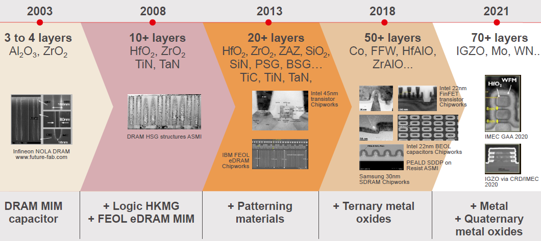
The technology is being applied in semi manufacturing at more layers with a wider variety of materials — in 2021 we had more than 70 ALD layers and this is now rising to above 80.
The below slide highlights all the areas in semi manufacturing where ALD is being used — simply put, it is seeing more and more applications:
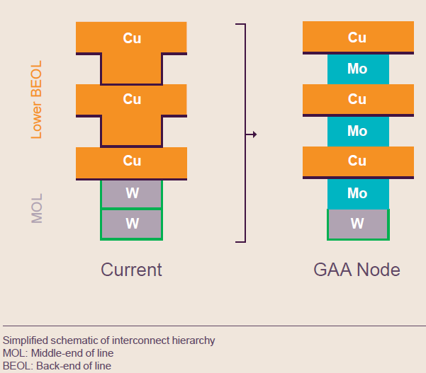
For example, due to the move to GAA, ALD will be used to replace some tungsten (W) and copper (Co) layers in the interconnect with molybdenum (Mo) ones:
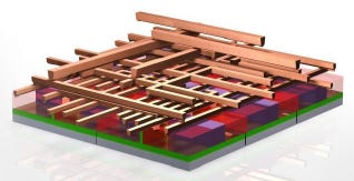
An illustration from Intel how metal layers can be architected to interconnect transistors:
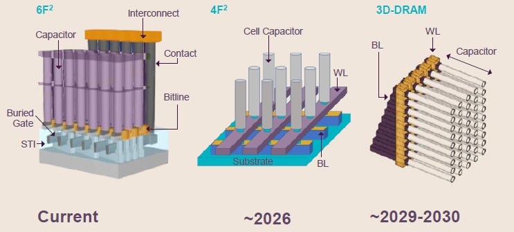
ASM’s head of products continued with the developments in memory: “So the industry is looking into how we can continue to scale DRAM. And the first thing is smaller cell sites, going from 6 f-squared to 4 f-squared. But at the end of the day, DRAM is going 3D, most likely by the end of the decade or earlier 2030s. Flash is the first technology that went 3D, and the scaling happens by adding more and more layers. Right now in production, there are 200-plus layers, and by the end of the decade, we’re going to have 1,000 layers for flash memory.”
Each DRAM cell can store one bit of data and is composed of one transistor and one capacitor. The cell orientation will see quite some evolution over the coming decade in 3D DRAM with transistors moving to a vertical stacking and the capacitors laying horizontally:
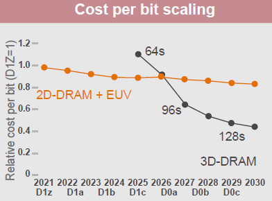
This move to 3D is currently the easiest way to increase the number of memory cells within a given chip area, resulting in a substantial decrease in the cost per bit. The timeline illustrated below has been pushed back a bit but it still gives an idea how the cost per bit can be reduced with more than 50%:
A NAND cell on the other hand has two gates, a control gate which is interconnected with the rest of the circuit and an isolated floating gate, which allows the cell to store a bit even when there is no power. Vertical cell stacking with 3D NAND is illustrated below — with in this case two tiers of 3D NAND cells being stacked on top of each other:
In this area, a nice application of ASM’s plasma enhanced ALD tools is the deposition of silicon oxide films to insulate the deep trenches between the layers of vertically stacked memory cells. Even a small void can cause electrical leakage leading to device failure. Another application in logic is depositing the through-silicon-via liner (TSV liner) on the right. As TSVs carry current between the different layers of a chip, they need an isolating layer around them.
Bringing this all together, below is an overview of the technology roadmap in all three, i.e. logic, DRAM, and NAND (flash):
What’s driving a lot of the above is what is called ‘selective ALD’, where — as the name suggests — deposition is happening only on a selected target area. ASM’s CTO detailed this at the 2021 capital markets day: “Litho-etch, that’s what we call top down. You pattern something, you etch out, and you throw away what you don’t need. That’s very inefficient. It’s much more efficient to grow things bottom up on the places where you want them. So that’s exactly what selective ALD is about. We can do this two different ways. Topological selectivity, which means that we only deposit on the flat surfaces and not on the side walls. And surface selectivity, where you deposit on a certain material and not on the others. Where are we here? We’re leading in the adoption of selective ALD. Topological selective silicon nitride is already in production in 3D NAND. And we have a joint development with an important customer for 2-nanometer foundry logic for what we call dielectric on dielectrics. So it’s a certain dielectric layer grown on dielectric and not on metal. And that eliminates a lot of edge placement errors. Selective ALD I think, really will present a very large SAM expansion for us going forward.”
Fastforwarding to 2023, the company has won two out of the three leading edge semi manufacturers which are moving to gate all around, and they mentioned they have ‘very good traction’ to win the third.
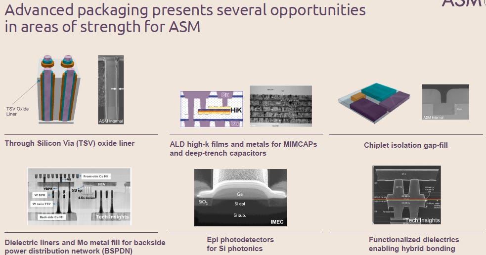
ASM is also seeing more ALD applications in advanced packaging, as well as with some of their other tools which will be discussed later. Together with scaling and 3D stacking, advanced packaging is really the other big trend currently in advanced semi manufacturing. As scaling is growing more expensive and there is no 3D stacking for logic (yet), multiple dies are being interconnected into one package to boost the computing power of the unit.
The company’s head of products detailed this: “So the opportunity we have in packaging, let’s start with the first one, this is through-silicon-via (TSV). The TSV needs oxide liner and very high aspect ratio. And what’s best, you deposit ALD with some of the plasma technology that I showed you earlier. The second thing is really looking into the MIM capacitors and the deep trench capacitor that actually are being used right now in the interposer. For this, we see many customers using our high-k ALD. The third thing is actually in the space of chiplet isolation. And the way to do it is to deposit very thick TEOS (a chemical), 40-micron thick. So that’s using the PECVD. The fourth is the backside power distribution network. Here, there are many ALD applications in the liners and also in the molybdenum fill. You can fill these aspect ratios with molybdenum and we have many new engagements in this area. Last but not least, hybrid bonding. This is really growing a lot and here, you need to have dielectric layers.”
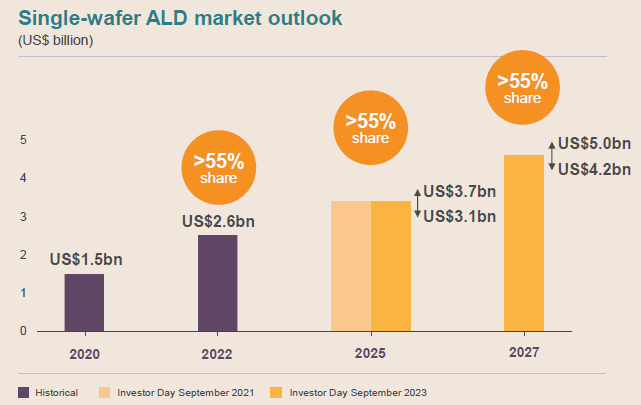
Overall, the company expects their core ALD market to grow at a double digit annual rate of around 10 to 14%, hitting around USD 4 to 5 billion in 2027 with the company expecting to maintain their 55% market share.
In the overall wafer fab equipment (WFE) market, GAA is expected to be the highest growth area. Memory (NAND + DRAM) is typically seen as taking up only around one third of semi capex going forward. Historically, memory’s share was larger, at around 40 to 50%. Logic is more capital intensive as its transistor architectures are already much smaller and with Moore’s law still progressing. Compared to NAND where the more asset-light vertical stacking is the name of the game. As a result, memory is currently only contributing around 19% to ASM’s revenues.
The company’s key competitor is Tokyo Electron (TEL) although also Applied Materials and Lam Research are looking to increase their share. All three of these are large semicap players which won’t make it easy for ASM. A factor which plays in ASM’s favor is that fabs typically have a dual sourcing policy, so a semi manufacturer doesn’t want to be fully reliant on say Applied Materials for its equipment. And it is in the interest of the fabs to have a sufficiently competitive environment among the tool manufacturers. However, on the flipside, if a tool manufacturer can create an integrated platform of multiple tools to significantly reduce to the total cost of ownership for the client (TCO - thus also including costs of operating the equipment), this will clearly be a factor that can allow it to gain substantial share. More diversified players such as Applied Materials and Tokyo Electron could have an edge here.
Yole shows a more competitive market than the company’s own calculated market share of 55%, however it seems they are lumping the above three markets together into one large market. Pilot equipment used in R&D won’t be a match for a high-volume TSMC fab.. However, even on both analyses, ASM clearly has a good position in what should be an attractive market in semiconductors.
ASM’s product portfolio
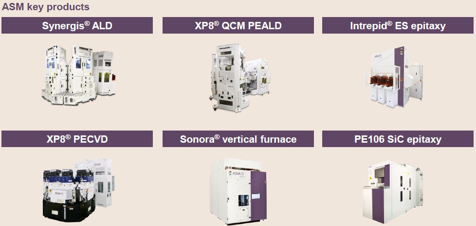
ASM has a variety of deposition oriented tools — not only ALD and plasma enhanced ALD, but also epitaxy (more on this in a bit), plasma enhanced CVD and vertical furnace. The advantage of plasma enhanced deposition is that this technique can be used at lower temperatures and as such is able to handle a wider variety of materials. Plasma is a gas that has been ionized, meaning that its atoms have been stripped of one or more electrons, leaving the gas with a net positive charge. This will make the gas highly reactive with its surrounding materials. The traditional ALD on the other hand is also called thermal ALD, meaning that it makes use of heat to create the desired reaction in the materials. CVD is basically an earlier generation of deposition, creating thicker coatings.
Their PECVD tools are more of a niche application where the company is seeing growth as the technology will replace spin-on-carbon at smaller transistor architectures. This is a smaller part of the business.
ASM claims to be the market leader in 8 inch (200mm) vertical furnaces as well. As SiC semiconductors are manufactured on these types of wafers, the company expects to have good cross-selling opportunities between their epi tools and vertical furnaces here.
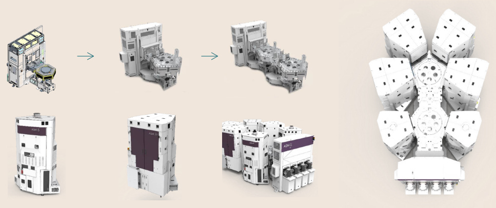
The company also has an integrated platform which can take care of multiple steps in one go — i.e. cleaning and different types of ALD enabling the deposition of a variety of materials. This can be done by different reactors such as those shown on the bottom left, and which now also got merged into the supertool on the right.
ASM’s head of products gives some further details: “So as you can see, we have a large portfolio of ALD products. But what’s common between all this ALD technology is that we have our unique reactor technology. One, we can achieve a uniformity of 0.3 angstrom on a very thin 48 angstrom film. The second thing is that the reactor is made to deposit up to 6 elements. This is important because Moore's Law is being driven by new materials. Third for the ALD technology is that we have very fast cycling times.”
Clarifying the last point he makes, the atomically thin layers with ALD are formed by alternating firstly precursors and then oxidants into a reactor chamber while purging out the by-products in between. These cycles are repeated until the desired film is deposited. So obviously fast cycle times will be crucial here.
An overview of epitaxy
Epitaxy (epi) is a special form of chemical vapor deposition (CVD) where a crystalline layer is deposited on top of another crystalline surface. For example, an additional thin layer of silicon can be deposited on a silicon substrate, or a layer of gallium nitride (GaN) can be placed on top of the silicon. This process can be used to create the source, drain and channel of a transistor. As transistors are moving towards smaller features, the number of epi steps has been on the rise in semi manufacturing.
In the construction of GAA transistors, epi is used to create the multi-layer stack of silicon and silicon-germanium nanosheets in the channel. Obviously this is very precise work and the ability to control the materials’ purity, thickness and smoothness are crucial.
ASM’s head of products detailed this: “As you can see in a FinFET, the channel thickness is defined by litho and etch. So you deposit your silicon, you litho it and then you etch it, which forms the channel thickness. If you flip that around by 90 degrees, you get the gate-all-around. So right now, the epi is actually what defines the structure. That means that epi thickness is very important as we can control the channel thickness one monolayer at a time.”
IEEE Spectrum as usual gives some very insightful background here: “The main trick is in building what’s called a superlattice, i.e. a periodic and layered crystal of two materials. In this case it’s silicon and silicon germanium. After the appropriate number of layers are grown, we use a chemical that selectively etches silicon germanium but does nothing to silicon, leaving only the silicon nanosheets suspended as bridges between the source and drain. Once you’ve got the silicon nanosheet channel regions constructed, it’s a matter of filling in the gaps, surrounding the channels first with dielectric and then with metal to form the gate stack. Both these steps are done with a process called atomic layer deposition, introduced in semiconductor manufacturing only a little over a decade ago. The process is so precise that the thickness of the deposited material is controllable down to a single atomic layer. One of the astounding things about the nanosheet design is that it may extend Moore’s Law so far that it actually outlasts the use of silicon in the channel. One potential solution is to introduce new materials into the channel region, such as germanium or semiconductors composed of elements from columns III and V of the periodic table, such as gallium arsenide. Electrons can move more than 10 times as fast in some of these semiconductors, allowing transistors made from these materials to switch faster. More important, because the electrons move faster, you can operate the device at a lower voltage, which leads to higher energy efficiency and less heat generation. Chipmakers have gone to great lengths to keep the heat down — clock rates don’t exceed 4 gigahertz. And the processor industry moved to multicore designs. If we ever want to be able to ramp up clock speeds again, we’ll need more energy-efficient transistors than silicon by itself can deliver.”
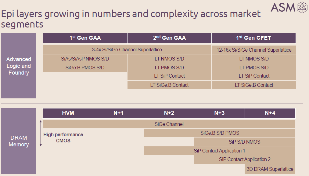
ASM gave the following overview of how they see the number of epi layers evolving in advanced logic and DRAM:
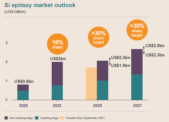
Although the wider epitaxy market isn’t expected to be a high growth area with a more modest 5% CAGR, ASM sees lagging node capex here falling back with stronger growth coming from increasing investments at the leading edge. Due to this transition to GAA, ASM is expecting their market share to grow from 16% to over 30%. They’re currently a smaller player at the lagging nodes, and as they’re looking to compete with their epi tools at the leading edge, they are seeing strong potential for market share gains. I’m doing some back-of-envelope maths now — combining these share gains with the mid single digit market growth rate, the company is actually guiding this business to grow at a 19% CAGR.
The company’s head of products detailed this further: “When you go to advanced CMOS, epi has to be deposited at much lower temperatures than power electronics — at 700 degrees Celsius. For power electronics, you have to deposit film at over 1,000 degrees. So at this low temperature, the surface on which the epi sits is not very clean — you can have oxide or carbon residue from etch, you can have defectivity. So in order for us to deposit pristine film, we have to remove this impurity. And that’s why we have developed an ALD-based surface clean technology. This reactor will monolayer by monolayer remove any defectivity before we deposit epi. We cannot break vacuum because if you break vacuum, then you’re going to have some oxide on your wafer again. So we came up with a platform, which allows us to integrate both the preclean and also the epi deposition into one platform.”
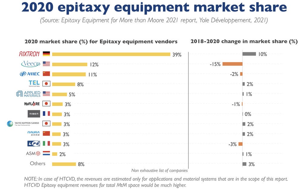
The overall landscape in the epitaxy market according to Yole is shown below. However, note that some of these players are purely focused on lagging nodes. Aixtron for example had historically high exposure to the LED lighting market, and going through their recent conference call, they now have high exposure to the SiC and GaN markets. So it probably would be better to try to subdivide this wider market into its niches. SiC equipment won’t be relevant to compete at 2nm GAA manufacturing for TSMC.
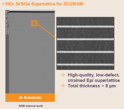
Another area where epi will be applied is in 3D DRAM, which will contain hundreds of silicon on silicon-germanium layers:
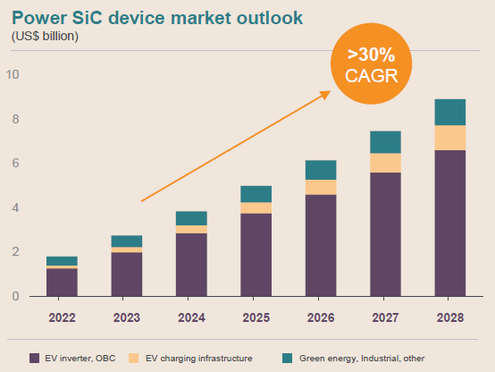
ASM also made the acquisition of LPE last year, an Italian company active in epitaxy for SiC wafers. This is a high growth market as SiC-based semiconductors are widely used to drive the transition to new green technologies such as electrical vehicles and green power generation (wind and solar). ASM saw LPE as having state-of-the-art technology and so they decided to put EUR 470 million down for the company.
ASM’s head of products seemed very enthused here: “We all know right now in electric vehicles, you want to do fast charging. So epi needs to be thicker. Also in solar energy we have inverters, and the solar energy is going from 1,000 volt to 1,500 volts. So right now, you need epi as thick as 100 micron. But it’s very difficult to deposit 100 micron epi in one step. And this is the capability of our reactor.”
We got an update on this business at the Q2 results, ASM’s CEO: “Since the acquisition of LPE, this activity has developed in a very positive way. Demand continues to be strong. Our team remains focused on ramping manufacturing despite supply chain constraints, which are still more challenging in this high growth part of the market. With a further increase expected in the second half, we are confident that our silicon carbide sales will increase to more than EUR 130 million (5% of revenues). The transition from 150 to 200 millimeter wafer sizes offers opportunities to step up our market share. We have practically engagements with almost every silicon carbide manufacturer in the world. We mentioned a couple of months ago about the first North American customer win and right now we have won a major European customer. Both are amongst the leading players in silicon carbide.”
He also discussed ASM’s general acquisition strategy at the capital markets day: “Last year was the first time in 18 years that we made acquisitions in this company. And we did two acquisitions, Reno Sub-Systems in March and LPE in October. Going forward, M&A will be an opportunistic growth opportunity, but we are also very focused. We will only look at acquisitions that are in the deposition space, either equipment or a technology that boosts or enhances our equipment.”
Reno is a smaller acquisition which provides tech to generate plasma.
The current competitive landscape
At the Credit Suisse conference, ASM’s CEO gave an update on the competitive dynamics in the industry: “Our competitors have been making announcements about some wins that they may have in the ALD space. Of course, there’s going to be some wins, some losses. But overall, if we look at 2-nanometer, we are very confident we will maintain our leading position.
If you look at our history, we started in ALD much earlier than anybody. And over the two decades, we have developed a lot of expertise in terms of chemistries, precursors and materials. So we have become the broad-based ALD player. In other words, we can play in all the different applications ALD serves today. Our competitors came late into the game. So they have been able to develop applications that serve a specific part of the market. And from node to node, not everything changes. So those things that don’t change, they just carry forward, that is already secured for us. So the competition is really in all the new applications that come about at a new node.
Epitaxy is a different story, here we are the follower. So we are up against a competitor that has a significant part of the market. We know the only way that we can win is if we have a good technology. We had our breakthrough with the leading fab at 7-nanometer and that’s continuing. Last year, we announced a second advanced win. So today, we have two customers, but we are involved with all three of them at 2-nanometer gate-all-around development. And we do expect to win some of the layers.”
Chinese export ban risk
Obviously there is a risk of export bans into China. ASM’s CEO discussed this at the Q2 results: “Let me now provide you with an update on our business in the Chinese market. A meaningful part of our power/ analog and wafer business is generated in China and this was again a very strong market in the second quarter. We have been successful in winning seven new customers in power/ analog in the last few years, which is now translating into significant revenue increases. We also serve China in the relatively advanced markets.
In October last year, the US government issued export controls basically targeted at the 40 nanometer and below nodes. We previously communicated that these controls would have a 15% to 25% negative impact on our China sales. Recently, the Dutch and the Japanese government also issued new export control measures. In terms of financial impact, we don’t expect a meaningful additional effect from these measures.
Following the export controls, a number of customers in China have redirected their strategy towards the less advanced nodes. As part of that, investments picked up in nodes such as 22 nanometer and 28 nanometer and this also contributed to our higher sales in China in the second quarter.”
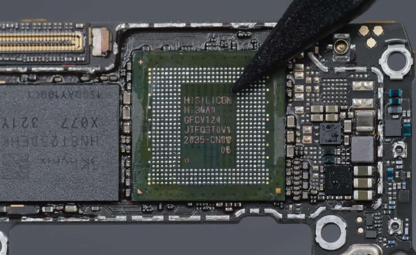
However, with the launch of Huawei’s latest phone on SMIC’s 7nm node, we know now that some of these tools have gone into advanced fabs as well — 7nm is only two generations behind TSMC’s 3nm node which is currently in the process of scaling up.
SemiAnalysis analyzed SMIC’s 7nm capacity — this is a great Substack to subscribe to, I’ll wait here for a moment.
“While we can’t validate these claims from China, it does appear to be very easy for SMIC to ramp to 30k WPM of actual production in their 7nm fab, without taking tools from other trailing edge fabs. Even with 50% yields, 30,000 WPM could support over 10 million Nvidia H100 GPU ASIC dies a year. No equipment used for advanced packaging similar to CoWoS or High Bandwidth Memory (HBM) is currently limited either. The cat is already out the bag in terms of capacity.”
Given that US export restrictions have failed at preventing China from building up advanced semi capacity, there is a likely risk that more severe restrictions are to follow of which more ASM tools could be a part. China is around 20% of ASM revenues currently so naturally this would be a blow.
The semi cycle
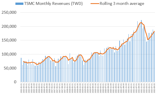
After the covid semi boom, the industry has now moved into a downcycle:
However, green shoots are emerging, TSMC’s monthly revenues over the July - September months have regained an upwards trajectory. Although the obvious risk is that a coming recession will send them southwards again. Economists have been calling recession since the start of last year and with US treasury rates currently having moved up to about 4.6% I’ll suspect they’ll likely be right at some point.
ASM’s CEO discussing the environment on the Q2 call: “Our leading customers continue to execute on their technology road maps and we confirm their timelines with regards to the upcoming gate-all-around node. We expect the first meaningful gate-all-around orders in the fourth quarter of this year for pilot activities planned for 2024. The introduction of gate-all-around in high volume manufacturing by the leading customers is still expected to be in 2025.
In the memory sector, market conditions continued to be tough in the second quarter as memory prices remain under pressure and manufacturers further reduce volumes to address excess inventory levels. Capex is currently limited to some modest technology investments. While we benefited from such investments, particularly with high-k metal gate for high-performance DRAM, the related volumes are relatively small. Our overall memory sales were substantially below last year’s sales and that is also what we expect for the second half. Consensus is that you are going to see memory sales starting to recover and that perhaps Q2, maybe even early Q3 is the trough. But let’s not forget that the memory manufacturers still have a lot of capacity today that they can just turn on and ramp up.
The trend in the power-analog sector remains solid and we expect continued strong performance in the second half. Demand in consumer applications further weakened in the second quarter, but this was again offset by continued robust demand in the automotive sector. We mainly play in these markets with our vertical furnaces and part of our epi portfolio.”
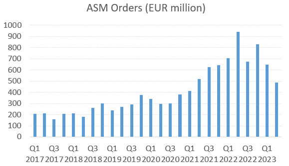
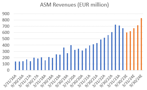
The company guided for orders to start increasing sequentially as from Q3, so reading through the above this will come from power-analog as they sounded very cautious on memory. As from Q4, initial logic orders to start GAA pilot lines should begin to help. The transition to GAA in the semi industry should be the next big driver for ASM’s order flow with the three leading players — TSMC, Samsung and Intel — building out their 2nm fabs. Currently lead times are around six months. The sell side is expecting ASM’s revenues to bottom this quarter, which might be a bit optimistic. Long term, orders will come in but in the near term there are quite a few wildcards with further possible Chinese export bans, the exact timing of initial GAA orders, and the overall macro environment.
Financials — current share price of EUR 395 on the Amsterdam Stock Exchange
The company is currently investing in both an R&D and manufacturing center in Dongtan, South-Korea — about twenty kilometers from Seoul. These works should be completed by 2025. While a recent expansion of the main manufacturing facility in Singapore has already been completed which should allow the company to fulfill demand in the coming five years.
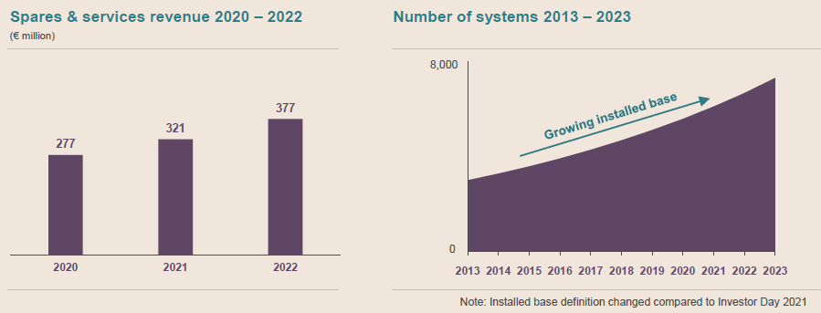
One of the most interesting businesses for the semicap players is the servicing of their equipment in the field, whereby they guarantee tool uptime for their customers and thereby bringing in recurring revenues. This much less cyclical business contributed 16% to revenues last year.
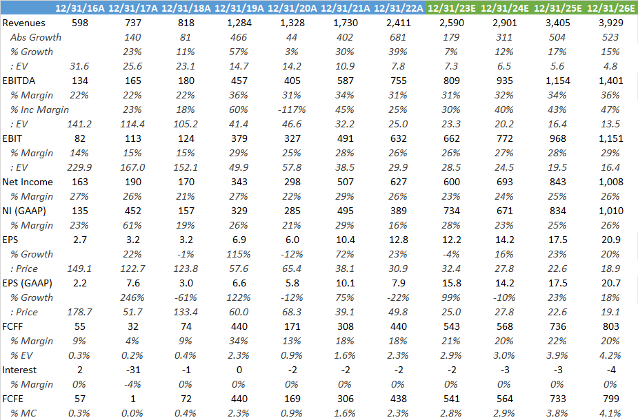
The sell side’s estimates below. This is not a cheap stock at 30x PE but should give you double-digit top line growth and higher EPS growth in return over the coming years. The current FCF yield is around 3%.
Compared to peers, ASM together with ASML is weathering the current downcycle best in terms of revenue growth.
The company has been trading around 28x next-twelve-months’ EPS on average over the last three years:
Long term model
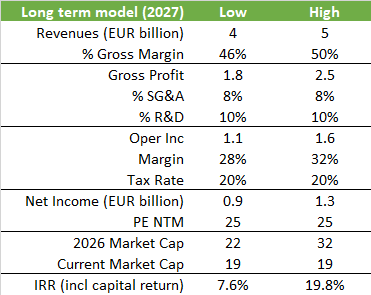
The company disclosed a number of target metrics for 2027, putting these into a model you can reach the following estimates. Naturally these have to be taken with a grain of salt although historically several of the large semicap players such as ASML have been providing excellent guidance. I’ve told you previously the story how everyone laughed when ASML said they were going to do EUR 10 billion in revenues long term but they’re going to do EUR 28 billion this year.. All the bears have long been buried. I’m less familiar with whether ASM International has been providing solid guidance but obviously the company has been executing well, going from EUR 600 million in revenues in 2016 to EUR 2.6 billion this year. And there should be a growth path for the company beyond 2027 with the move to CFET transistors in logic and 3D RAM in memory. Putting the 2027 projected net income on 25 times would give an IRR of around 8% under the conservative scenario and nearly 20% under the bullish scenario.
What are the risks to obtaining these IRRs?
The main risk is if technological transitions in transistor architectures slow down. This is the main source of order flow together with capacity expansions. So if this source falls away, numbers will disappoint. A healthy cadence in the progression to next-gen nodes is really vital for this stock to work.
Although Tokyo Electron is currently the main competitor, also Applied Materials and Lam Research are looking to grow in ALD. ASM looks to be having a very comprehensive portfolio in this field, but over time competitors will be able to expand their offering as well.
Another risk is Chinese competitors continuing to progress with the production of also more advanced tools. These are still quite behind at the moment but that could start to change within five years or so, which would put pressure on ASM’s multiple and order flow.
Overall, this is a fairly interesting name which could bring in attractive returns for long term investors. In the near term there are some risks to the share price such as when exactly we’ll find a bottom in the semi cycle and possible further export bans in the US - China chip wars. And with interest rates now at fairly high levels, there is also substantial risk of a broad macro slowdown in the coming twelve months which would impact the semiconductor sector as a whole.
If you enjoy research like this, hit the like button and subscribe. Also, please share a link to this post on social media or with colleagues with a positive comment, it will help the publication to grow.
I’m also regularly discussing tech and investments on my Twitter.
Disclaimer - This article is not a recommendation to buy or sell the mentioned securities, it is purely for informational purposes. While I’ve aimed to use accurate and reliable information in writing this, it can not be guaranteed that all information used is of this nature. The views expressed in this article may change over time without giving notice. The future performance of the mentioned securities remains uncertain, with both upside as well as downside scenarios possible. Before investing, I recommend speaking to a financial advisor who can take into account your personal risk profile.












🔥🔥
Traditionally, atomic layer deposition has been a very slow process. If this is still the case, ALD will not scale to high volumes, and thus, the output will never get to economies of scale.