ASML held its investor day recently, where the headline was that the company reiterated its long term revenue outlook, bringing relief to the market after the recent 2025 downgrade and the company’s weak order intake over the last year(s).
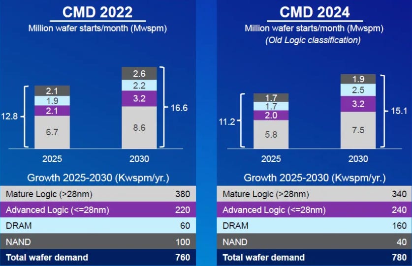
However, under the hood, ASML is seeing quite some shifts happening in the semi industry with the rise of AI. Most notably in memory, due to the intensity of volatile memory in datacenter GPUs, ASML strongly upgraded the growth outlook for DRAM wafer volumes over the coming six years. At the same time, NAND wafer growth saw a strong downgrade:
While ASML is seeing a bullish outlook for semiconductor revenues overall, most of this growth is expected to happen in high-performance-computing applications, i.e. AI:
And a lot of this growth will continue to take place in the cloud, with both AI training and inference servers driving the attractive CAGR in the datacenter semis market:
As AI servers are both DDR and HBM intensive, this drives the strongly expected growth in the number of DRAM wafers mentioned above:
However, the more important side of the equation for ASML is scaling. To accomplish transistor shrinkage, both more fab processing steps and more complex processing steps are needed, raising the need for more lithography tools and more advanced ones. This phenomenon is also called Rock’s Law, i.e. the increasing capex required to keep up with the transistor scaling of Moore’s Law.
Another way to look at Rock’s Law is the rising cost per wafer node-on-node, which has been a huge tailwind for ASML and the semicap industry:
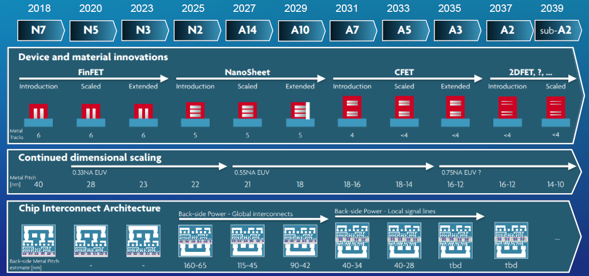
And also here ASML gave a bullish outlook, with the Angstrom era to start in 2027 and then the introduction of CFETs early during the next decade. Where the latter could even create the need for a new hyper-NA tool, especially to deal with the rising densities in the interconnect.
Below is the industry’s estimated trendline for scaling the metal pitch in logic semis, with the pitch shrinking a few nanometers at each new node. For high-NA, ASML’s next-generation EUV tool, the company sees insertion opportunities already at the first Angstrom node in ‘27. This is as A14 will require an increasing need for double exposures with low-NA EUV in a single processing step, raising costs. Multiple litho exposures and the accompanying additional processing steps with other tools such as etch are also called multiple patterning, so there’s double patterning, quadruple patterning etcetera, depending on the number of repeated exposures you have to do to complete the processing step. With high-NA EUV on the other hand, double EUV exposures can be accomplished in a single step.
Below is an illustration of how a chip circuit can be created with both low-NA EUV and high-NA. In low-NA EUV, for this example three exposures are needed. So the wafer needs to go undergo the litho-etch process twice, after which some final cuts are made with another etch step. In high-NA on the other hand, the whole pattern can be printed in a single exposure:
As single patterning with high-NA requires less non-litho steps, ASML sees the capex intensity for these steps shifting towards lithography. Basically the high-NA tool will require more capex and bit more litho opex, but lower non-litho costs:
So for the industry to scale towards A10 in 2030, there are two ways to do this. The first option is multi-patterning with traditional EUV, which would see EUV usage rising from around 20 exposures per wafer in 2025 to 25-30 exposures in 2030. However, the company is expecting that around 5 high-NA layers will be adopted by 2030, which is the second option. This would reduce the need of traditional EUV by 10 layers, as high-NA can replace low-NA usually at a 1:2 ratio. The graph on the right for DRAM follows the same logic, EUV usage will continue to climb and also here ASML is expecting 2 to 3 layers to be done with high-NA.
The chart also shows how DRAM is much less litho intensive than advanced Logic. However, with the strong growth in DRAM wafer volumes, ASML is expecting EUV spend for the DRAM industry to grow at an even faster rate than in the Foundry market. So the company is expecting an EUV CAGR of around 20% for DRAM compared to around 15% for Logic.
Needless to say this is a bullish outlook for ASML’s highest growth business, EUV. Last year, EUV contributed around 33% to ASML’s revenues:
This is ASML’s CEO Christophe Fouquet on the outlook for ASML and the lithography industry:
“We believe that lithography will remain at the heart of our customers’ innovations. If you need more advanced process, lithography today is still the best way to drive down costs. I know some of you had doubts about the weight of lithography moving forward, but this weight will not only remain strong, it will continue to grow. We can scale EUV for many, many years.
A few years ago, customers were not even sure they will need a 2-nanometer node. Who can afford it? That's only 3-4 years ago. There was then a risk that the whole roadmap will slow down. If you hear the story today around AI with our foundries' customers, those AI customers are extremely eager to get 2-nanometer chips and they will be equally eager in the future to get 14 Angstrom chips because that's the only way to really address costs and power consumption. So AI will again demand an acceleration of the roadmap and that's creating an opportunity for higher performance tools in lithography.
That's the story for logic, but what's happening in DRAM is also interesting. High-bandwidth memory today is the bottleneck of AI. But HBM is only the first step, what we believe will happen moving forward is processing-in-memory (PIM). This means that in memory, we will see logic coming together with DRAM to improve performance and reduce power consumption. So we expect a major shift on the DRAM roadmap. Memory is the market that will be the most affected in a positive way by AI.”
For premium subscribers, we will go much deeper into current developments for ASML and in leading edge semis. We’ll focus on topics such as the future of EUV, high-NA, the future of memory, ASML’s strategy in metrology, the long term financial outlook for investors, and Fouquet’s bear case..


