


ASML High-NA Deep Dive and which Stocks to Play if TSMC postpones Adoption
A tour of current developments in High-NA

Introduction
Moore’s law — the doubling of the number of transistors every two years which can fit into a given chip area — has been primarily driven by improving resolutions in the field of photolithography, the realm where monopolist ASML dominates with its advanced immersion and EUV tools. The field of photolithography is basically the activity of exposing light through a reticle onto a silicon wafer, so that circuit patterns can get patterned into the photoresist film. Subsequently, these exposed regions are etched away in an underlying layer, giving form to the integrated circuit.
Over the years, litho tool manufacturers had two main ways to progress to finer resolutions: 1) decreasing the wavelength of the lightsource, and 2) increasing the numerical aperture (NA) of the projection optics, for example, by making use of better lenses or even inserting a liquid between the wafer and the lens (immersion litho). Finally, we have various other process specific improvements which can help such as better techniques involving the photomask — through which the light passes — as well as computational lithography which makes use of advanced algorithms to implement all sorts of optimizations.
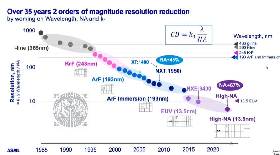
The progress made by ASML and its various litho tools over the years are illustrated above. All these tools are still in use today, even the old ones, both to manufacture older style chips (mature nodes) as well as to pattern the less advanced layers in a state-of-the-art GPU. The current workhorses of advanced semi manufacturing are the immersion tools (ASML NXT series) and naturally the most advanced EUV tools (ASML NXE series). When you want to build a current leading edge fab, you needs loads of both of these.
As markets and analysts where still pondering a decade ago now, whether EUV could be turned into a reality some day, ASML started work on its next-next-generation High-NA system with a targeted release date in 2024. Given how EUV had been postponed for over a decade at that time and had become a true nightmare for the company, with loads of bear cases from critics flying around and investors asking why they were throwing so much money away, it’s remarkable that here we are in 2024, and the high-NA tool is ready as scheduled.
Let’s have a look how ASML accomplished this remarkable feat. Over the 2014-2018 period, the company spent four years designing the whole high-NA system. The system would be built up from four separate modules, which could be designed, manufactured, and optimized individually by separate teams.

From 2018 to 2021, manufacturing sites to build the system were installed on four locations: the reticle is manufactured in Wilton, Connecticut, the source is manufactured in San Diego, the optics in Oberkochen, Germany together with Carl Zeiss, and the wafer handling is manufactured in ASML’s hometown of Veldhoven in the Netherlands.
Starting from 2020, the company embarked on integrating these manufactured modules into a complete high-NA system. Each module underwent its own tests with final individual qualification.
Only recently, around Christmas time of last year, the final piece of the puzzle was completed and the entire high-NA system received qualification. This first tool was shipped to Intel so that Pat Gelsinger could start putting together his new tool in the company’s R&D fab in Oregon.

Four months later, Intel was finishing up on getting the system ready:

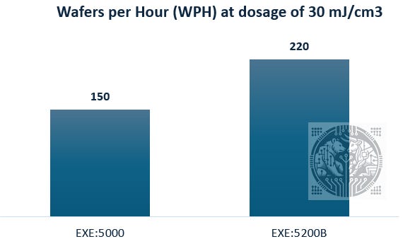
The other remarkable feat of high-NA is that the productivity of the tool is impressive already, with the current version processing 150 wafers per hour (WPH) and which will increase to 220 WPH next year:
This is in stark contrast to EUV, the tool was barely running a decade ago — processing a mere 20-30 wafers per hour, at a feeble light source, and with lots of downtime:
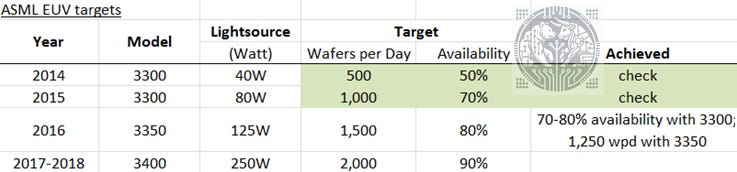
As already mentioned, this was a nightmare for ASML at the time given that these were the results of a tool which was ten years late, and naturally plenty of bear cases were flying around that the tool would never make it. Additionally, only sporadically a limited amount of orders for the tool were coming in. If the tool was so highly desired by TSMC, Samsung and Intel, why weren’t they placing orders?
Perhaps all this might sound familiar to today, the current bear thesis on high-NA is basically the same as it was on EUV a decade ago: “the productivity is too low”, “orders aren’t coming in”, widespread reports that TSMC wants to go with multi-patterning instead, and even ludicrous reports that the foundries are waiting instead on ASML’s next-next tool (hyper-NA).
For premium subscribers:
We’ll contrast and compare the current situation in high-NA with how EUV grew into a success.
We’ll have a detailed look at the current data and research on high-NA tools using a variety of sources.
We’ll go through how the leading edge value chain is currently working on high-NA insertion.
We’ll highlight three stocks to play if the industry postpones high-NA adoption for one or more nodes.
We’ll walk through how ASML investors (and short sellers) should think about developments going forward.