A Primer on the Deposition Market, and a Deep Dive on the High-Growth ALD Market
The Outlook in the ALD Market, Kokusai vs ASM, and New Competition
A Tour of the Deposition market in Semi Manufacturing
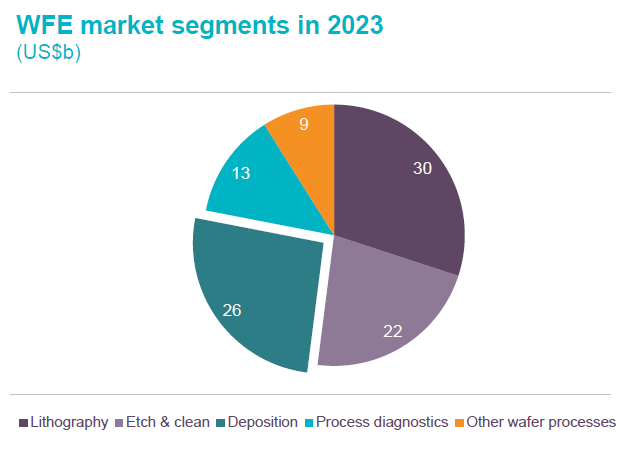
Deposition is one of the three big processes in semi manufacturing. These days, a wafer in leading edge semi manufacturing undergoes more than a thousand processing steps in a fab, and a very typical processing cycle entails deposition - lithography - etch. In deposition, thin films of materials are added on top of the wafer. Subsequently, the needed chip pattern is projected onto the wafer with ASML’s lithography tools, after which the exposed underlying materials are etched away to create the desired pattern. Wafers are shuttled between the various types of tools in the fab via the overhead transport system.
The wafer fab equipment (WFE) industry is expected to grow at a high single-digit CAGR as chip architectures continue to increase in complexity, both in logic and in memory. This increasing chip complexity requires more processing steps with more advanced tooling, increasing the capex required to construct a leading edge fab.
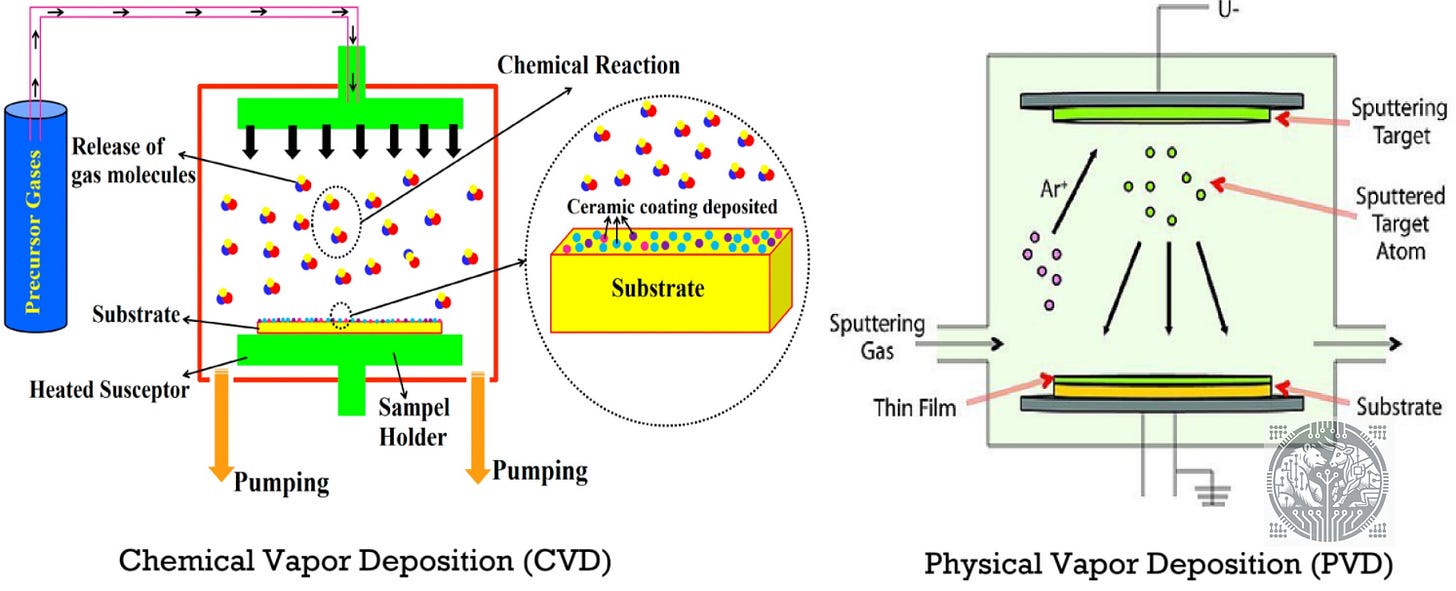
There are four key types of deposition technologies. Thirty years ago, chemical vapor deposition (CVD) and physical vapor deposition (PVD) were the two key types, however since then, a number of other types were introduced as wafer processing continued to grow in complexity. Initially, Applied Materials was the dominant player providing this equipment. The company has to this day very good CVD and PVD systems.
Then, Novellus Systems came in and developed a series of deposition platforms to become a credible competitor. Novellus was later acquired by Lam Research, the champion in etch, with the aim of broadening out its product offering. This way, the company became a more serious competitor to the more diversified equipment providers such as Applied Materials and Tokyo Electron.
Each of the new players which emerged in the WFE industry gradually built out their product portfolio over time. For example, Novellus initially competed in plasma enhanced CVD while Japanese players such as Tokyo Electron and Kokusai initially focused on low pressure CVD. A variety of deposition and etch techniques are needed to handle the different material types involved in chip construction. The competitive race in WFE equipment gave rise to ever better performing tools with a lower total cost of ownership.
In the late ‘90s, copper electroplating became a critical new segment in the deposition market. Copper started to replace aluminum as the preferred metal to interconnect chip components. Aluminum layers were deposited with PVD, but as this process was not precise enough for high-aspect ratio chip features which were being introduced alongside copper, a new type of deposition had to be developed. The expert in electroplating techniques was IBM, which continues to be a key research lab for the semi industry to this day, so Novellus Systems licensed this technology to become the champion of electroplating.
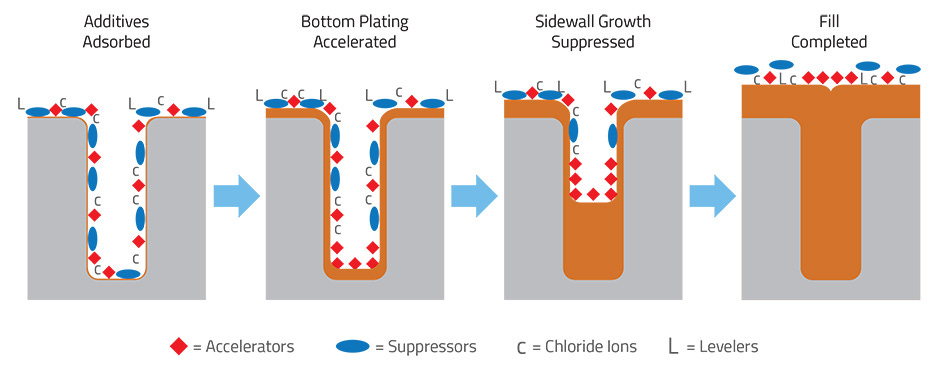
The latest development in the deposition industry is atomic layer deposition (ALD). With ALD, material layers with a thickness of one atom can be uniformly deposited over chip structures. In the early 2000s, ALD was first introduced to coat DRAM capacitors as CVD had become inadequate. Later on, in order to scale towards 45nm, also the logic industry started to struggle with classic deposition methodologies. This is when Intel introduced ALD to construct the high-k metal gate (HKMG) transistor. Previous silicon-based gates had started to cause current leakage at this smaller scale, creating the need to introduce new materials and provide better insulation.
So in the late 2000s, also ALD became a critical deposition process. Although CVD and PVD remain the larger markets up to this day. CVD and PVD continue to be used for less critical layers, even in advanced semi manufacturing, while layers where the highest precision is needed are done with ALD. For example, to to deposit thicker insulators or to create an epitaxial layer onto a wafer, these are still done with CVD, while thicker metal chip layers are manufactured with PVD.
So throughout the chipmaking process, layers of insulating and conducting materials are deposited. The insulating layers are also called the dielectrics while the conducting materials are metals such as copper or tungsten. To handle each different type of material, a specialized process has to be developed by the equipment provider. And the chemicals involved in these processes can be part of the IP of the equipment provider.
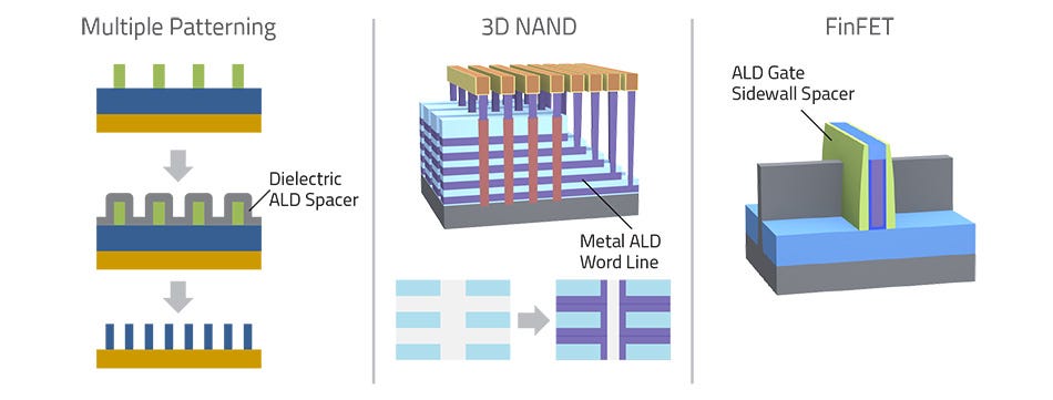
Semi Engineering illustrates logic and memory processes where thin films are deposited with ALD:
Even when TSMC moves to a new node, often around 90% of the manufacturing process stays the same. This means that the tool manufacturers which were used at the previous node will again see new orders coming in. This is why there are usually no sudden dramatic market share shifts amongst the equipment providers, even in more competitive areas of the market. It’s only for the parts of the manufacturing process that are novel that there is an opening to take share. TSMC’s next node at 2nm will bring in a larger change as usual as we move from the FinFET era into gate-all-around transistors.
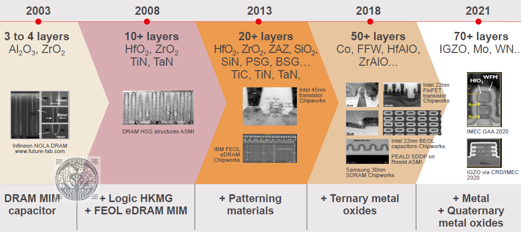
As transistor architectures are growing in complexity, i.e. with smaller features making use of a wider variety of materials, ALD has been an attractive growth market over the last few decades. Ever more chip layers are making use of the technology:
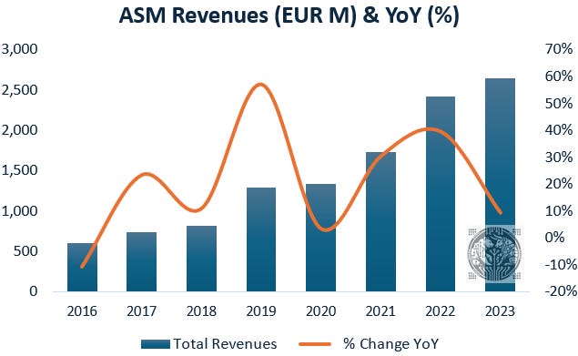
Which led to an attractive growth story for ALD equipment manufacturer ASM International:
In this article, we’ll go deeper into the two ALD specialists, Kokusai Electric and ASM International. We’ll also review current developments from competition such as Applied Materials and Tokyo Electron, which are aiming to gain share in the attractive ALD market. And we’ll give the insights from former and current directors at leading companies in the semi industry such as Intel, TSMC, Applied Materials and ASM to get a deep understanding of the market and its outlook. These industry experts are available via Tegus. Finally, we’ll analyze the financials and valuations of companies in the space and discuss key stock picks.


